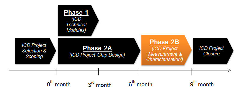
Phase
2B – Integrated Circuit Design Project ‘Measurement &
Characterisation’
Key Deliverables – Yield
enhancement & Design improvement
Duration: 3 months
(i) A good post-layout simulation result does not necessarily
warrant a successful product. In reality, the actual performance
of the IC can only be ascertained by carrying out measurement
and testing of the IC hardware returning from the fabrication
facility. In the measurement and testing step, the fabricated IC
prototype or the packaged IC is subject to rigorous electrical
and functional measurement and testing on top of specification
checks. If the measurement result is not on-target, the
designers need to perform troubleshooting or debugging of the IC
to identify potential technical flaws. All design specifications
must be met before proceeding to the packaging.
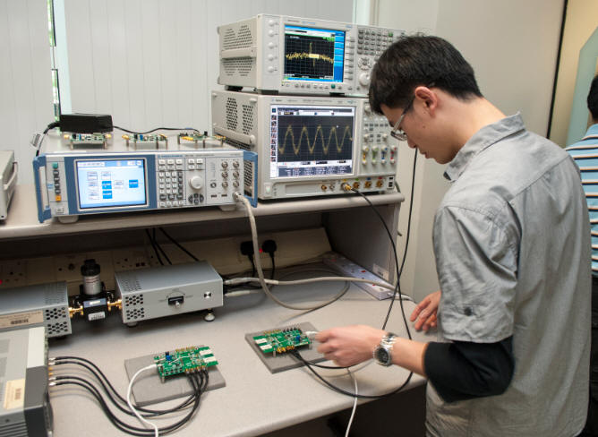
(ii) In order to ascertain if the IC meets the electrical
specifications, state-of-the-art equipment such as 12” probe
station, semiconductor parameter analysers, precision LCR
meters, network analysers, high frequency noise parameter
systems, load-pull systems, 1/f noise systems, jitter/bit error
rate testers, function generators and oscilloscopes are needed
to perform the necessary measurements.
(iii) Some ICs may have to be mounted on printed circuit boards
for additional testing.