Key Deliverable – Schematic Diagrams (GDS file)
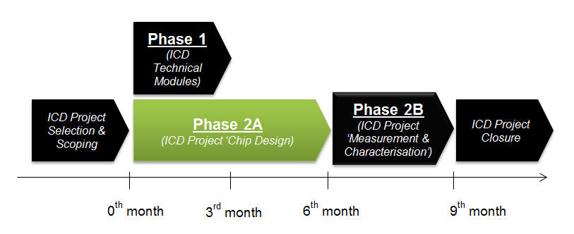
Duration: 6 months
(i) Design specifications based on specific
engineering requirements and system criteria.
(ii) Design on a two-dimensional transistor-level circuit
diagram/description, or circuit design in short,
constructed using a CAD tool (e.g., Schematic Editor from the
Cadence Virtuoso framework). Besides designing circuits in
graphical form, circuit description may also be prepared in
written format, commonly known as a netlist using a CAD tool
such as HSPICE from Synopsys.
(iii) The schematic diagram or netlist then undergoes
circuit-level simulations (e.g. Cadence’s Virtuoso Spectre or
HSPICE circuit simulator). This is followed by optimisation of
the schematic design.
(iv) The circuit schematic is converted into a layout comprising the
three-dimensional geometric artwork according to industry
standards.
(v) A parasitic extraction (PE) step followed by a verification
stage (i.e. layout versus schematic (LVS)) check is conducted.
(vi) A post-layout simulation is performed by designers to
evaluate the electrical performance of a full-custom IC design
based on the extracted netlist.
(vii) If the design meets all the specifications, the design
file typically in the form of GDS stream format is send for
manufacture. This process is widely referred to as design
tape-out in technical terminology.