Fig. 1 | Fig. 2 | Fig. 3 | Fig. 4 | Fig. 5 | Fig. 6 | Fig. 7 | Fig. 8 | Fig. 9 | Fig. 10 | Fig. 11
X. ZHOU and T. TANG
The EEE Journal, School of Electrical and Electronic Engineering, Nanyang Technological University
Vol. 7, No. 1, pp. 58-64, July 1995.
Abstract | References | Citation | Figures | Back
A single-engine multi-level simulator, with automatic circuit partitioning, dynamic parameter extraction and mode switching, is described. Its application to modelling GaAs heterostructure field-effect transistor digital circuits is demonstracted in terms of device-, transistor-, circuit-, and gate-level models.
Fig. 1 | Fig. 2 | Fig. 3 | Fig. 4 | Fig. 5 | Fig. 6 | Fig. 7 | Fig. 8 | Fig. 9 | Fig. 10 | Fig. 11
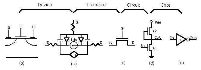
Fig. 1 Multi-level representation of an HFET.
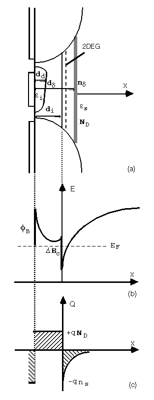
Fig. 2 The modelled HFET: (a) cross-sectional view, (b) band diagram, and (c) charge distribution.
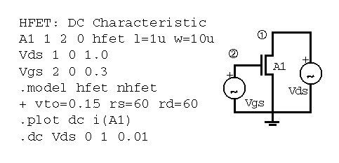
Fig. 3 The netlist and the circuit for simulating the HFET DC characteristic,
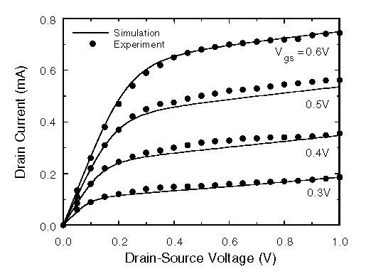
Fig. 4 Simulated DC characteristic (solid lines) and compared with experimental results (symbols).
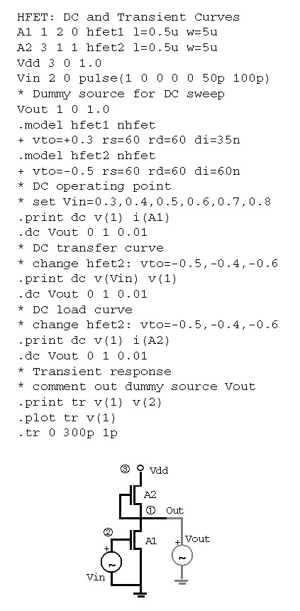
Fig. 5 The netlist and the circuit for simulating the HFET inverter DC operating point and transfer curve, as well as transient response.
Fig. 6 The calculated HFET E/D inverter DC characteristics with load lines (at different threshold voltages for the depletion-mode transistor).
Fig. 7 The calculated inverter transfer curves (at different threshold voltages for the depletion-mode transistor).
Fig. 8 The calculated inverter transient response.
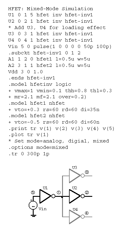
Fig. 9 The netlist and the circuit for mixed-mode simulation, showing the effect of fanout.
Fig. 10 The calculated transient voltages at the output of U1 for different loads (broken line: one gate; solid line: two gates; dotted line: three gates) in three simulation modes as indicated.
Fig. 11 The calculated transient voltage at the output of U2
for different loads (broken line: one gate; solid line: two gates; dotted
line: three gates) in three simulation modes as indicated.