Tianwen Tang and Xing Zhou
School of Electrical and Electronic
Engineering, Nanyang Technological University
Nanyang Avenue, Singapore 639798,
Republic of Singapore
Abstract | Figures | Reprint | Back
(Click on the Figure inside the Paper to see its enlargement.)


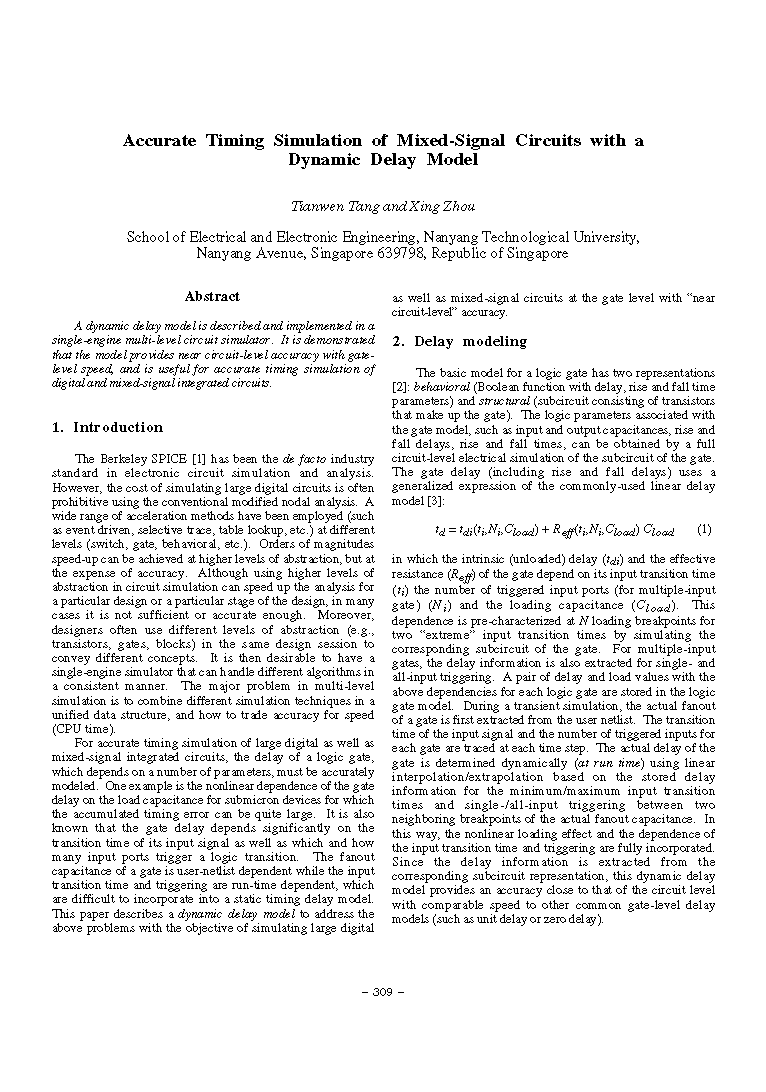
Fig. 2 Voltage waveforms at node 1 of the circuit shown in Fig. 1 with different loads and different simulation modes.
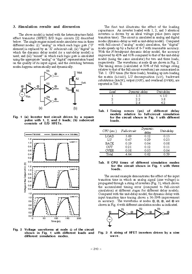
Fig. 3 A string of HFET inverters driven by a sine wave.
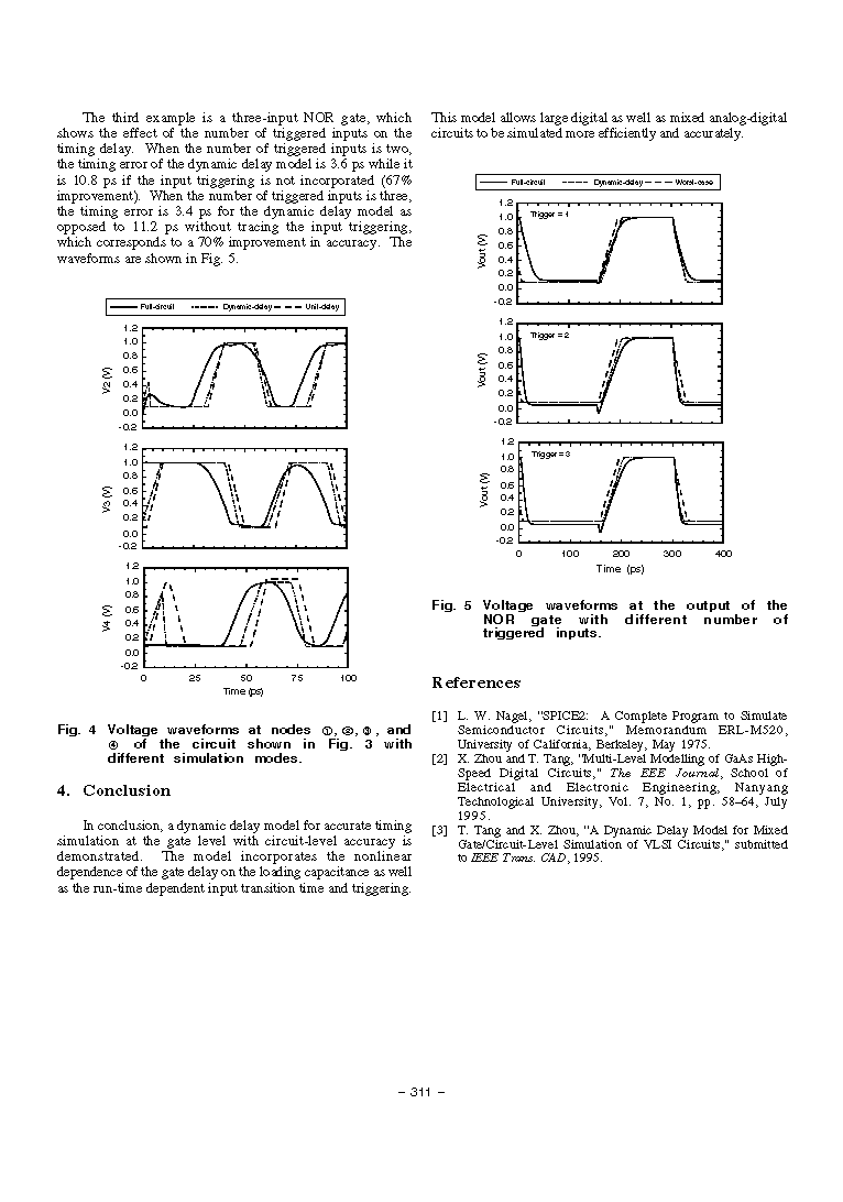
Fig. 5 Voltage waveforms at the output of the NOR gate with different
number of triggered inputs.