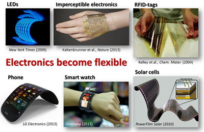
Printed electronic devices have changed the way we think about electronics application in our day-to-day life. This has shown significant social and economic impact in the recent years. Our group have made a lot of efforts in developing ink formulations and processes for the application in printed electronics, which consist of the following materials: (i) metal nanostructures (Cu, Ag), (ii) semiconducting polymers (PEDOT:PSS, P3HT:PCBM) and (iii) semiconductor nanostructures (CdSe, CuS/ZnS/SnS2, Cu2ZnSnS4 and CuIn(S,Se)2).
Highlights
Conductive ink
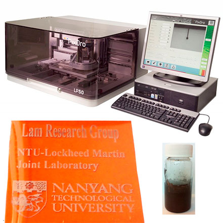 Our group have developed a stable conductive ink-based on Cu nanostructures (NanoCu) and these Cu nanostructures could be in the form of nanoparticles, nanowires, nanoplates or a mixture of any of the above shapes. The ink can be sintered at relatively low temperature (100 oC ~ 200 oC) to obtain good conductivity. The resulting Cu thin film exhibits very good mechanical flexibility on flexible substrate, with less than 20% change in resistance after 1000 cycles of bending test. The NanoCu ink is able to form conductive lines/films that could be used as interconnects in PCB board, electrodes in solar panels, antenna and RFID application. This project is developed in collaboration with Lockheed Martin Co.
 |
|
 |
 |
Nanoparticles ink based thin film solar cell
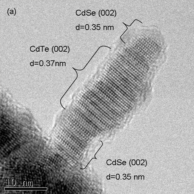
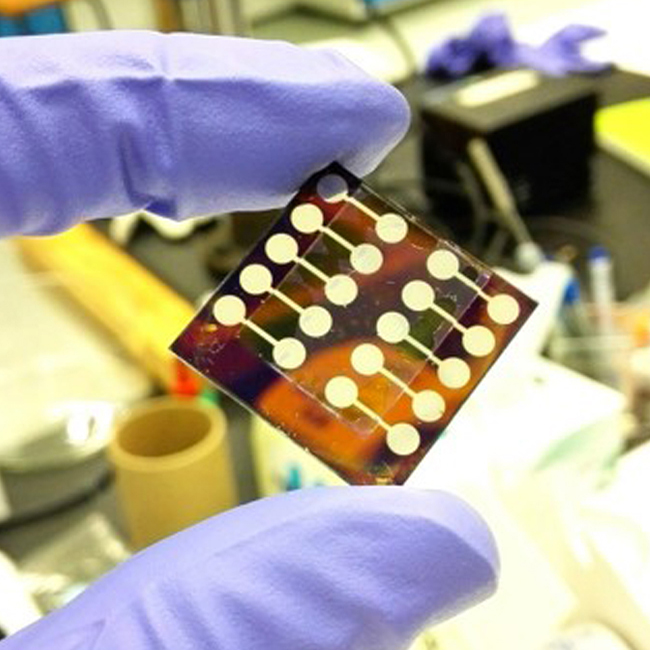
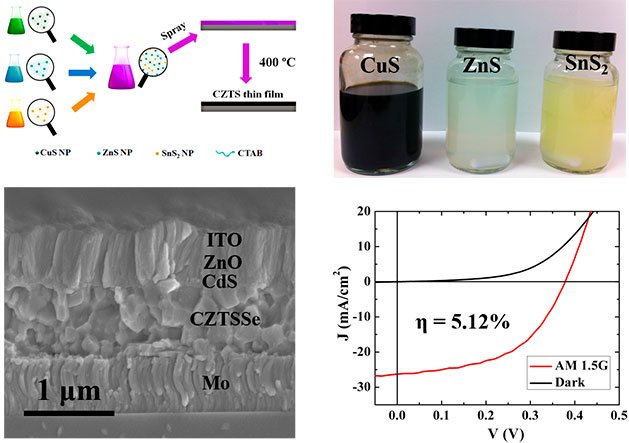
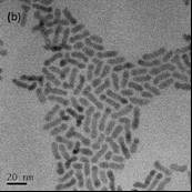
Quaternary CuInGaSe2(CIGS) and Cu2ZnSnS4 (CZTS) are promising absorber materials for thin film solar cells. We have demonstrated a low cost, environmentally friendly ink formulation to prepare CZTS film using aqueous systems. The thin film solar cells were fabricated following Mo/CZTSSe/CdS/ZnO/ITO/Au architecture, and an efficiency of over 5% have been achieved. In addition to above formulation, we have also develop solution based synthetic routes to obtain nanostructures of a range of semiconducting materials – CIGS, CZTS, CdSe, CdTe and CuIn(S,Se)2. This can be in the form of nanoparticles, nanorods, nanowires and other form of nanostructures. We were also able to also synthesize heterogeneous nanostructures. All these structures formed a good dispersion in appropriate solvents and used in solar cells applications.