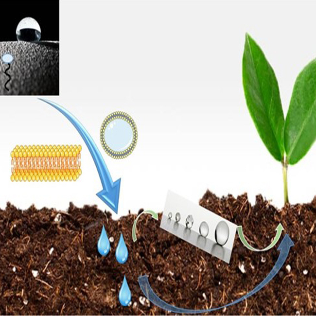
Materials characterization is an essential component in the research in our group. Characterization provides an insight into the structure-property relationships and the underlying mechanisms, which are of utmost importance as we develop novel materials, alter them into different structures and incorporate them into various applications. This is made possible by our strong link with the world-class characterization facility, Facility for Analysis, Characterization, Testing & Simulation (FACTS), in our home institute. A few research areas that we are working on include the X-ray scattering and spectroscopy, electron microscopy and scanning probe microscopy.
Highlights
X-ray scattering and spectroscopy
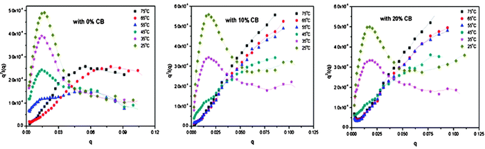
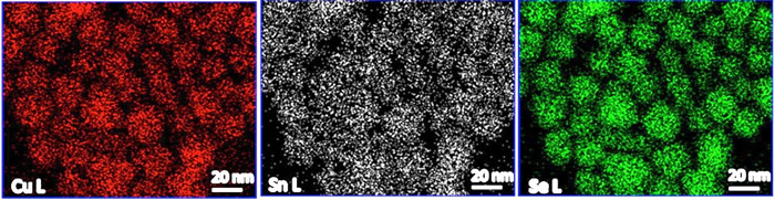
X-ray-based techniques are often used to provide the structural and electronic information of both crystalline and amorphous materials. X-ray scattering allows us to probe into the structural evolution of polymer nanostructures as they self-assemble in solution. On the other hand, X-ray spectroscopy enables the determination of the homogeneity of elemental distribution in our inorganic ternary nanocrystals.
Electron microscopy
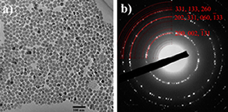
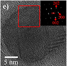
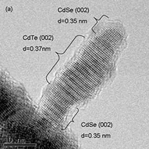
To complement the information elucidated from X-ray-based techniques, we use electron microscopy. Depending on the energies of the electron, we could probe not only the surface of the materials but also their bulk with electron microscopes, with resolution down to atomic scale. Electron diffraction also allows us to probe the local order in the nanostructures we have synthesized.
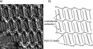
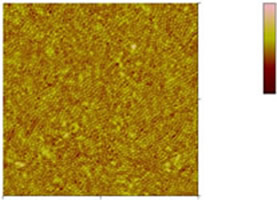
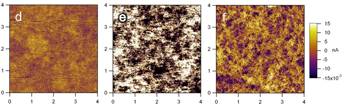
Scanning probe microscopy
The other characterization technique we often use to study our materials is scanning probe microscopy. In a typical experiment, imaging is done as a tip is brought in close proximity and then scanned across the surface of the sample. The tip-sample interaction will determine the type of information collected. We have investigated the molecular arrangement of organic molecules as they self-assemble on substrate with scanning tunneling microscope (STM). On the other hand, by introducing electrical current to the sample through the metal-coated tip, we were able to map the electrical conductivity within our sample.