E425: Engineering Design V
TCAD: Process and Device Simulation
X. ZHOU
©
1997
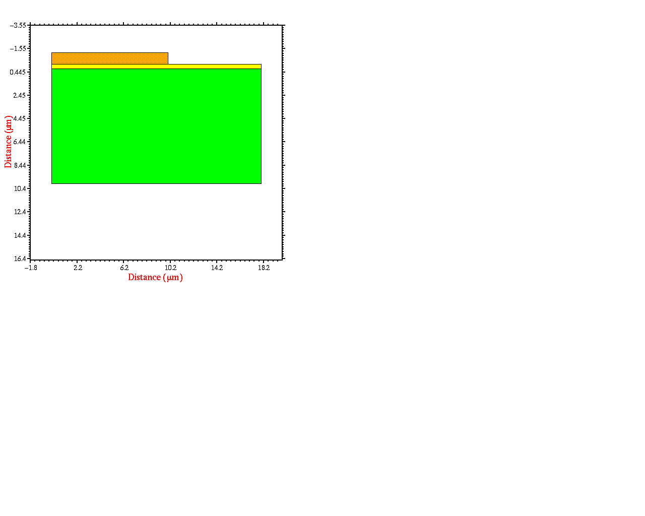
Step 3: Simulated Structure
Step 3:
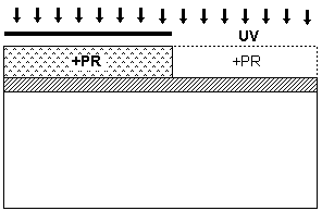
N-well photolithography
:
Mask: NWELL; Deposit positive photoresist (+PR); Masking; Exposure; Development.
Cross-Sectional View
Input Command
$step load_mask
mask in.file=layout:0_0.tl1
$step nwell_mask
deposit photo thick=1
expose mask=NWELL
develop