E425: Engineering Design V
TCAD: Process and Device Simulation
X. ZHOU
©
1997
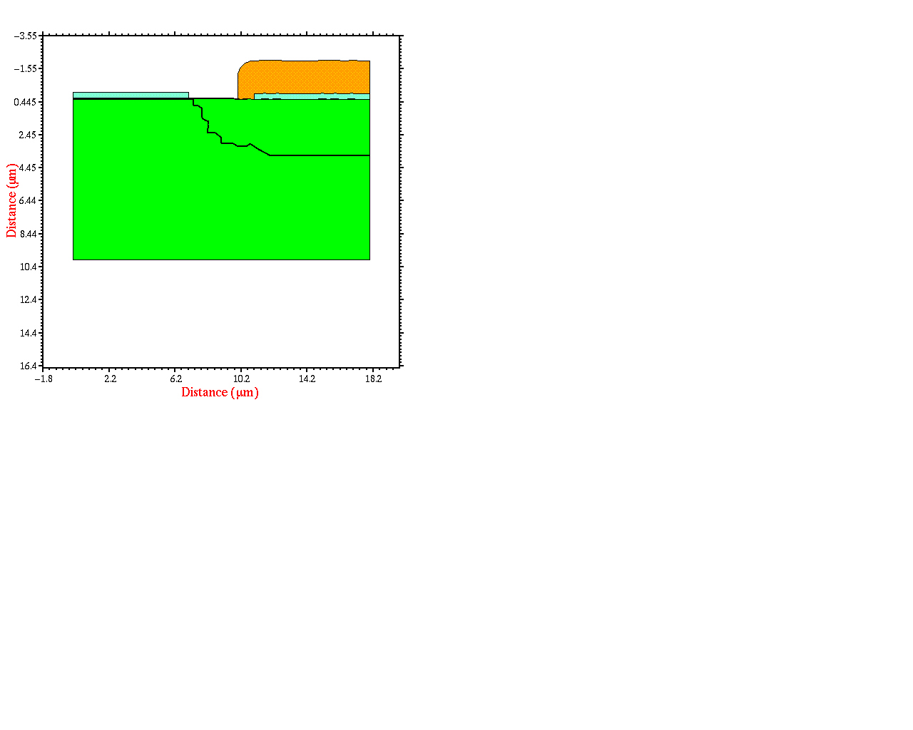
Step 13: Simulated Structure
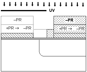
Step 13:
Field implant photolithography
:
Mask: NWELL; Deposit negative photoresist; Masking; Exposure; Development.
Cross-Sectional View
Input Command
$step pfield_mask
deposit negative photo thick=1
expose mask=NWELL
develop