One of the challenges of the deep-submicron technology is due to the
fact that as transistor dimensions are getting smaller, their performance
is more closely coupled with the fabrication parameters, and the interconnect
delay is becoming dominant. This means that the transistor structure
and processing information need to be considered in the early stage of
a design before it is fabricated. This new trend places demands for
new design methodologies as well as new design tools.
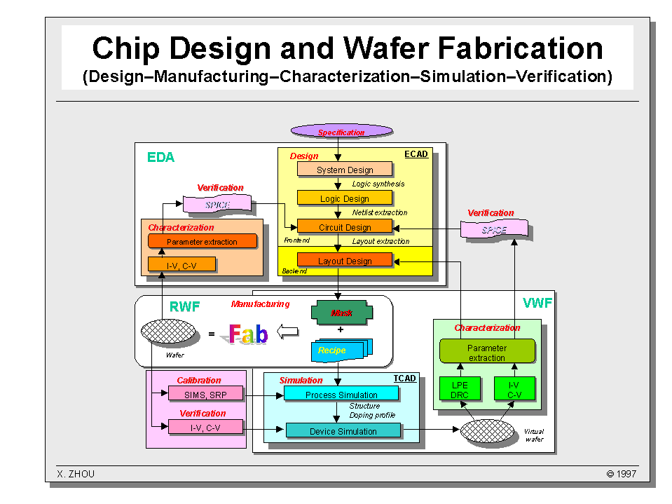
Chip Design and Wafer Fabrication
The semiconductor industry or, to a larger extend, the microelectronics industry, involves chip design and wafer fabrication, which is a complex, iterative process of design manufacturing characterization simulation verification.
A chip design starts with the product specification, followed by the frontend and backend designs. In this phase, ECAD tools have been developed so powerful that the logic design can be synthesized from a high-level hardware description language (HDL), the circuit netlist can be extracted from the logic functional description, and the layout can be extracted from the circuit- and logic-level descriptions.
Once a set of mask has been designed, it is combined with a given process recipe in the manufacturing phase in a real wafer fab (RWF). Electrical and technological characterization is then performed on the fabricated device to extract the parameters for back-annotation and verification.
Although the EDA tools (including design and verification tools) are already quite advanced, this design manufacturing characterization verification loop can be very costly if a first-time silicon success cannot be achieved. Moreover, it would be extremely expensive and time consuming if a new technology is to be developed using this iterative experimentation.
With the maturity of TCAD tools, real wafer fabrication can be emulated by process simulation, from which realistic device structures and doping profiles can be generated, and transistor performance can be characterized through device simulation with reasonable accuracy. Interconnect delays can also be extracted through technology characterization with 3D accuracy, which can provide information for design rule checker (DRC) and layout parasitic extraction (LPE) tools in the physical design. SPICE parameters can also be extracted from the virtual device IV characteristics for back-annotating circuit simulators and timing analyzers, which provides the notion of calibrating ECAD tools based on TCAD tools. It is obvious that there is great incentive to develop this virtual wafer fab (VWF) technology to supplement the RWF experimentation.
Of course, how effective this approach will be in aiding first-time
silicon success depends on how well the process and device simulators are
calibrated to the RWF results. This calibration involves another
loop -- manufacturing calibration simulation verification.
The process models must be calibrated to the experimental doping and carrier
profiles obtained from secondary ion mass spectroscopy (SIMS) and spreading
resistance profiling (SRP); and the device models must be verified with
the measured IV and CV characteristics.
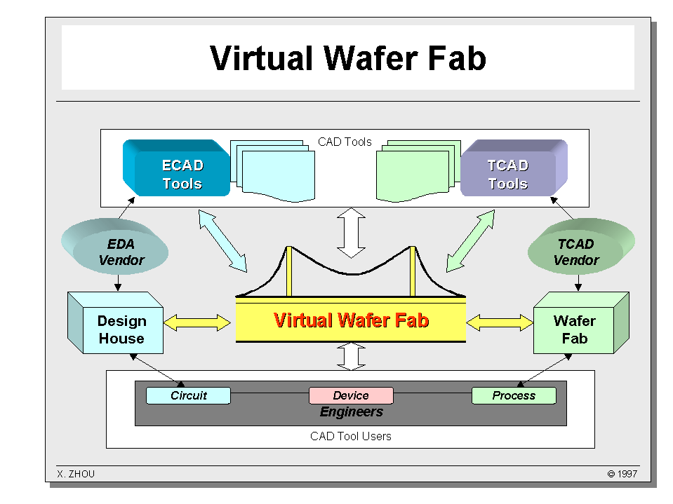
EDA vendors provide ECAD tools for the design house and TCAD vendors provide TCAD tools for the wafer fab. These tools are used by the designers (circuit, device, and process engineers), or collectively, the CAD tool users. The lost link between the design house and the wafer fab has not been significant before the deep-submicron era.
The notion of virtual wafer fab is to bridge the gap between the two.
This virtual wafer fab technology will be proven to be increasingly vital,
if not a must, in the deep-submicron ULSI era. Basically, it serves
as a bridge between the design house and the wafer fab, between the ECAD
and TCAD tools, and between the CAD tools and CAD tool users in general.
It will have a major impact on the way we develop a new technology.
It will eventually change the way we design in the same way as the EDA
has shaped the whole microelectronics industry.
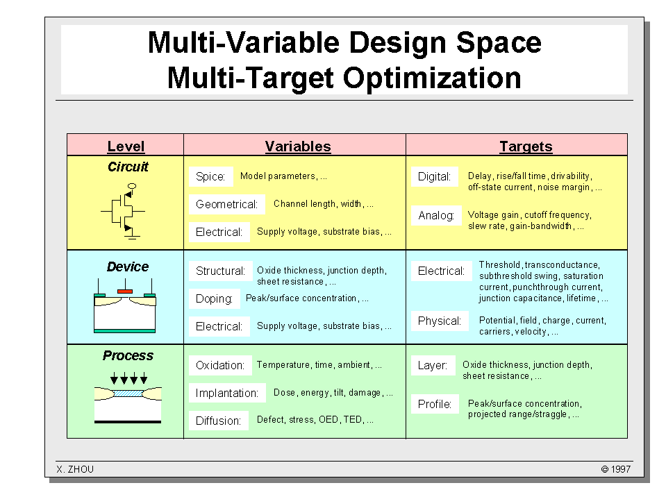
Multi-Variable Design Space, Multi-Target Optimization
The virtual wafer fab technology is based on the use of TCAD tools centered at the device level. The problem is very complex in the sense that it has a multi-variable design space and it is a multi-target optimization problem. Just take a process simulator as an example. For a particular process, there may be tens of different models to choose from, hundreds of parameters to adjust, and thousands of factors to influence the final outcome. In this sense, the question is not whether the tools can be used or not, it is how they should be used. TCAD should not be tweaking coefficients for all days. It should be used for testing concepts by analysis and design.
The multi-target optimization problem should be decomposed at different
levels: process, device, and circuit. The target values of a specified
gate delay, threshold voltage, or subthreshold swing, etc. depend on different
variables at different levels. Transistor characteristics are more
related to device parameters such as gate oxide thickness, junction depths,
effective channel length, etc., which are indirectly related to processing
variables such as oxidation time and temperature, implant dose and energy,
etc. It is important to break these dependencies at different levels
so that they can be tackled more accurately and efficiently.
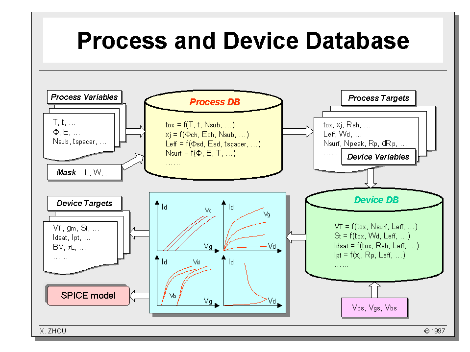
The first step is to identify target parameters to be designed or optimized. The specification will be different for different applications. For example, threshold voltage is one of the most important parameters in CMOS circuits, which is influenced by many variables. Any process variations, such as gate oxidation time or temperature, threshold adjustment implant dose or energy, will have direct impact on the final threshold voltage. However, from the device modeling point of view, it is the gate oxide thickness and the channel doping profile which influence the device electrical characteristics.
Hence, it is advantageous to construct separate databases for the processes
and devices. For the process database, the input will be the processing
variables and mask information, and the output will be the layer structures
and doping profiles. The database stores all the inputoutput dependency
data and, if possible, compact models linking the input and output can
be developed. The device database, on the other hand, takes the device
structure and biasing condition as input and stores the generated IV characteristics,
from which device targets can be extracted. Again, it would be extremely
useful and efficient if compact analytic models at the device level can
be developed based on the detailed TCAD results. Finally, circuit-level
parameters and interconnect delays can also be extracted from the virtual
device IV characteristics.
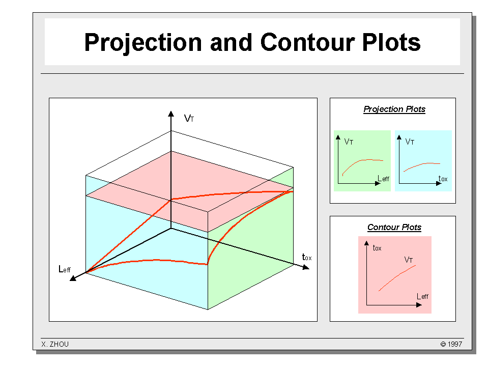
Once a complete process and device database is constructed, a specified set of multi-target objects can be readily accessible from the multi-variable design space. These targets can be visualized graphically by 3D plots, e.g., a plot of the threshold voltage (Vt) as a function of the effective channel length (Leff) and the gate oxide thickness (tox).
These 3D data can be viewed in different ways at the designers discretion. One type is the projection plot in which the target is plotted against one major variable, optionally with a secondary variable as a parameter. The other type is the contour plot in which constant values of the target are plotted against two major variables.
These plots can be generated directly from the database. If compact
models are developed, it would be extremely efficient to generate these
plots, which can be used for multi-target optimization.
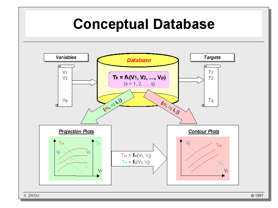
A conceptual database is described as one which stores the targetvariable dependency data in a form easily accessible to the user. Each target in the database can be related to a number of variables. These data are generated from a complete set of simulations based on the TCAD models, which includes all the nonuniformities in chemical/electrical distributions and the nonlinearities of carrier transport. Each targetvariable dependency represents a particular design of experiment (DOE). If a compact model is developed for a particular dependency, an analytic functional relation for that dependency is also defined.
Conceptually, data can be manipulated to obtain any view of a specified
target. For example, projection plots of the mth target as
a function of variable i for different values of variable j
can be generated at the choice (m; i, j), and the
nth target can also be plotted in the same way for comparison.
Likewise, by specifying the target values for the mth and nth
targets, contour plots can be obtained as a function of two variables i
and j. These plots and data can be used for nonlinear regression,
response surface modeling (RSM), and simultaneous optimization of multiple
targets.