Have you ever imagined this: Whenever you push the button of an electronic system (e.g., the keyboard of a computer, or the remote control of a VCR), you are actually manipulating the motion of individual electrons inside the system.
Since the invention of the transistor 50 years ago and the advent of
the modern VLSI technology, we have witnessed the dramatic advancement
in the microelectronics industry. It is all based on the foundation
of the semiconductor industry for our ability to make electrons move faster,
transistors smaller, and more transistors on a single chip. As this
trend leads us into the ultra-large-scale integration (ULSI) era, the deep-submicron
technology calls for new design methodologies and new electronic design
automation (EDA) tools to cope with the complexity and coupling among different
stages of a design.
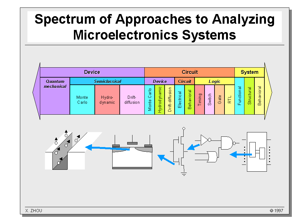
Spectrum of Approaches to Analyzing Microelectronic Systems
There exists a wide spectrum of approaches to analyzing microelectronic systems, which can be largely classified into three levels: system, circuit, and device, with the corresponding three walks of people: system designers, circuit engineers, and device physicists.
At the engineering end of the spectrum, system designers are concerned with the behavior and functionality of a complex system. In general, a top-down synthesis approach is employed in a system design. Design methodologies evolve with the rapid advancement of the technology as well as design tools. New approaches, such as semi-custom design (standard cell, gate array, field-programmable gate array, etc.) for the application-specific integrated circuits (ASIC), have been widely used. Nowadays, it is totally unimaginable that a Pentium chip can be designed bottom-up without the use of advanced EDA tools.
Traditionally, integrated circuit design has been centered at the de facto industry standard -- the Berkeley SPICE circuit simulator. Higher-level logic simulators (such as switch-level timing analyzers, gate-level or register-transistor-level simulators) are aimed at increased simulation speed at the expense of accuracy. On the other hand, circuit designers expect a set of SPICE parameters to be extracted from the lower layout or technology level for use in circuit simulation as well as logic-level verification.
For ultra-small-size transistors or non-steady-state transport problems,
the closed-form macromodels at the circuit level will not be sufficient
or valid for the analysis of the problem at hand. Device electrical
performance is characterized by 2D/3D numerical solutions of the coupled
Poisson and current continuity equations, together with the drift-diffusion
(DD) or energy-balance (EB) equations. When highly nonequilibrium
and nonlocal effects are of importance, Monte Carlo (MC) technique is used
to solve for the exact solution of the Boltzmann transport equation.
Finally, at the physics end of the spectrum, many attempts have been
made to formulate a rigorous theory of quantum transport.
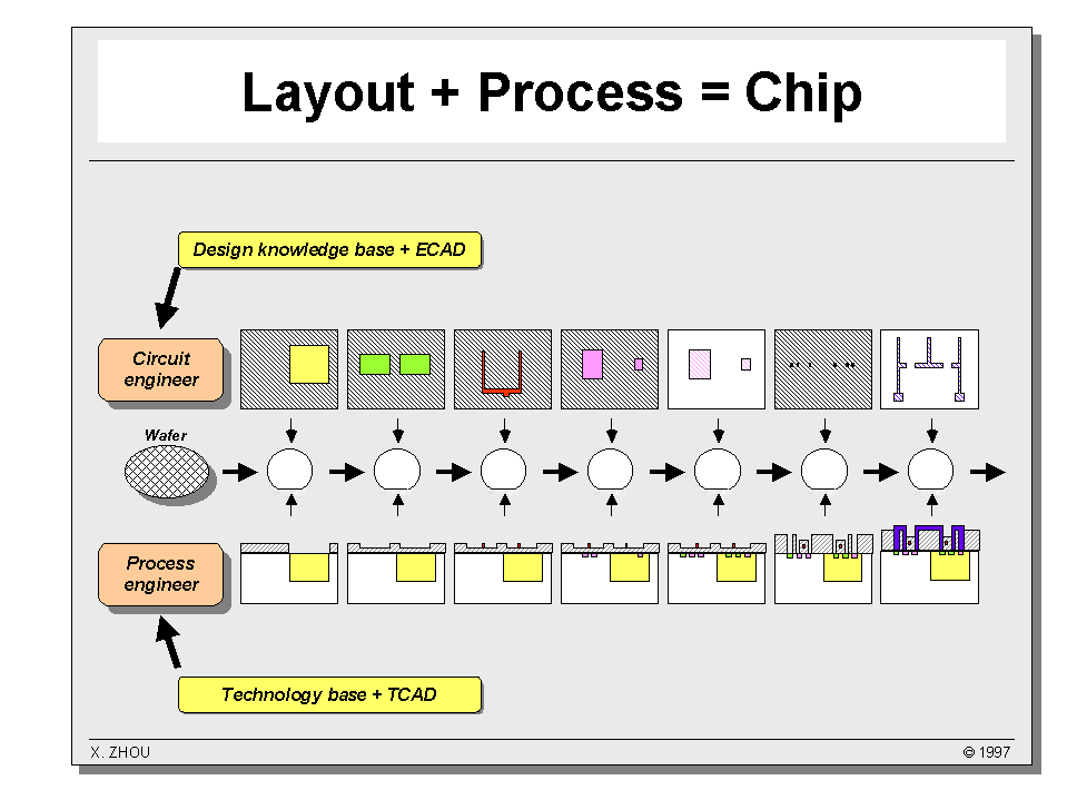
VLSI Design and Manufacturing Hierarchy
A microelectronic system, from concept to product, must go through the process of design and implementation. Before the deep-submicron era, a full-custom design (as opposed to other semi-custom ASICs) mainly consists of two sessions: frontend and backend.
In frontend design, it usually starts from the system level with a top-down synthesis approach, which is technology independent (i.e., at this level, it is irrelevant whether the design will be implemented in CMOS or bipolar technology). The design is then transformed into the circuit level, in which the logic functionality, timing delays, speed and power, etc., are the primary concerns. This level is technology dependent but relatively process independent. If more detailed study on the transistor performance is needed, it can be supplemented at the device level based on the device physics which, in general, requires process information.
At the backend, the final design must be translated into the physical layout representation, which is to be used to implement in wafer fabrication. In the conventional hierarchy, technology development (manufacturing) is relatively independent of the design. The feedback only occurs at the circuit level where the fab provides the circuit designer a set of SPICE parameters for the particular process through electrical measurement and parameter extraction of the fabricated transistors.
From the described VLSI design and manufacturing hierarchy, two streams
of knowledge can be identified: vertically, a single design is represented
at different levels of abstraction; horizontally, any design (in its final
layout format) must be combined with a process recipe to be implemented,
step by step, on a silicon chip.
The design and implementation of an integrated circuit, be it the whole system on a chip or a single inverter, can be represented at five distinctively different levels of abstraction (take the inverter as an example):
From another point of view, the final physical design (layout) of the
system must be implemented into the silicon chip (or committed to silicon).
This process involves the application of each individual mask during the
processing of the silicon wafer. Again, take the inverter as an example,
the final completion of the device consists of a sequence of processing
steps, such as diffusion, oxidation, and ion implantation, for a given
technology. The final performance of the system (the device) not
only depends on the physical design (layout), but also on the process in
which the device structures and doping profiles are altered. Imagine
that for the whole system, this combination of layout and process must
work laterally for all layers of the masks as well as vertically for
all layers of depths.
A new technology development is the process of achieving the optimum device performance through process variations. Generally, it involves three streams of knowledge: device physics, processing technology, and circuit design. It is centered at a specified process recipe since the final target is a process flow to implement the optimum design into the silicon chip. However, process variation must be constrained by the design rule and the scaling rule. The transistor electrical characteristics are closely coupled with the doping profiles and layer structures, and very often, trade-off must be taken for different design targets. Processing technology, such as the self-aligned technology, is also linked to the mask design and limited by photolithography.
Traditionally, technology development is relatively independent of the
circuit design. However, when going into the deep-submicron regime,
the conventional scaling rule does not apply any more. Device performance
is closely coupled with the fabrication parameters and circuit design constraints.
Circuit designers also need process information (such as interconnect delays)
at the very early stage of the design. Many of the conventional scaling
rules and design methodologies are changed.
Traditionally, the microelectronics industry consists of two major sectors: the design house where chips are being designed by system/circuit engineers, and the wafer fab where chips are being fabricated by process/device engineers. In a design house, extensive electronic computer-aided design (ECAD) tools supported by the EDA vendors are used. A design session generally involves an iterative process from logic design (frontend) to physical design (backend). In a wafer fab, expensive equipment from the equipment vendors are used to fabricate the chips. The primary concerns are things like design for manufacturability, statistical modeling, sensitivity analysis, yield and reliability, all supported by computer integrated manufacturing (CIM).
The link between the design house and the wafer fab has been the mask information (GDS II files) and a set of SPICE parameters. The design house provides the mask information for the wafer fab, and the fab provides the SPICE parameters for the particular process to the design house. However, the SPICE parameters, which are needed in the circuit design, will not be available before the device is fabricated. For deep-submicron technologies, this information and, in particular, the interconnect delay information, is critical at the very early stage of a design (before fabrication).
With the rapid advancement of process and device models, technology
computer-aided design (TCAD) tools are developed by the TCAD vendors to
emulate wafer fabrication and device characterization. Realistic
process information (layer thickness and doping profiles) can be obtained
from process simulation, and electrical information (IV and CV characteristics)
can be obtained from 2D device simulation. Then, SPICE parameters
can be obtained through parameter extraction based on the simulated electrical
characteristics, and delay information can be obtained through technology
characterization. So far, the TCAD approach to technology development
and transistor design has been widely used by all semiconductor companies,
but it is mainly restricted to the device engineer and R&D community.