 |
|
Multilevel Modeling of Nanometer CMOS ULSI Systems Based on a Compact Model and Single-Engine Simulator Xing Zhou School of Electrical and Electronic Engineering
|
 |
|
|
|
The past three decades have witnessed dramatic advancements in integrated-circuit (IC) technologies, from small-scale integration (SSI) to today�s ultra-large-scale integration (ULSI) with multihundred-million transistors on a single chip. Accompanied with these advancements is the evolution of advanced models and simulators at various levels of abstraction that are used to design and simulate these ULSIs. The electronic design automation (EDA) industry has been driven by the ever-increasing demands of the IC design and manufacturing. To cope with increasing speed and complexity in digital, analog and mixed-signal circuit simulation, a hierarchy of simulators and algorithms, together with generations of device models, have been developed, such as event-driven logic simulators, switch-level timing analyzers, analog behavioral languages, lookup-table approaches, hardware description languages (HDLs), and hierarchical circuit simulation. Each approach is targeted to its own problem domain, and a combination of these available tools has been the practice of the IC design and design automation industries over the past decades.
As we are entering the nanometer ULSI era, conventional approaches to circuit design and modeling become questionable or even invalid. A static timing analyzer may give wrong delay estimates since interconnect delay becomes dominant, which is layout-dependent. Event-driven digital simulation based on latency becomes questionable since some subcircuits that are supposed to be functionally latent might be electrically active due to variations in the power rails or small crosstalk coupling signals. With system-on-chip (SoC) designs, mixed-signal circuitry becomes inseparable and a major part of the design that requires analog accuracy while still demanding digital speed for large-block or full-chip simulation. Circuit designers now rely more on feedback from technology developers for the device models as the effect of process fluctuations on circuit performance becomes significant in nanometer designs. These are all well-known problems for the design and EDA communities. The solutions to these problems, however, are nontrivial not only because of the complexity of the problems but also due to the maturity of existing simulators and device models. The entrenchment of established approaches and routines as well as standardization of popular models have made it very difficult for new models/approaches to get accepted [1]. As a result, efforts are being made to add all kinds of nanometer effects to those popular models and implement them in major commercial simulators, which makes them more complex and less unified and consistent.
This article reviews the trends and needs in multilevel modeling in the context of nanometer CMOS ULSI systems, with an emphasis from the model/tool developer�s perspective. A dual representation of transistors/circuit is proposed and demonstrated through physics-based compact modeling and single-engine circuit simulator based on subcircuit expansion. Extension to process correlation and block-level representation is also proposed, which will be the key to studying process effects on system performance. This consistent dual representation allows detailed physics captured at a lower level to be propagated to the higher level of abstraction. The key idea is to build a physics-based device compact model (CM) based on technology characterization, which serves as the building block for an implicit multilevel circuit simulator based on subcircuit-expansion approach. In this way, process variation can be captured through device CMs, and its effects on circuit/system performance can be linked to a consistent hierarchy of abstractions within the same simulator engine.
Hierarchical Modeling
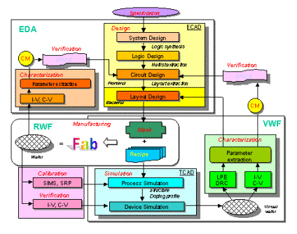
The semiconductor industry or, to a larger extent, the microelectronics industry, involves chip design and wafer fabrication, which is a complex, iterative process of �design - manufacturing - characterization - simulation - verification.� A chip design starts with the product specification, followed by the front-end and back-end designs. In this phase, electronic computer-aided design (ECAD) tools have been developed which are so powerful that the logic design can be synthesized from a high-level description language, the circuit netlist can be extracted from the logic functional description, and the layout can be extracted from the circuit- and logic-level descriptions. Once a set of masks has been designed, it is combined with a given process recipe in the manufacturing phase in a �real wafer fab� (RWF). Electrical and technological characterization is then performed on the fabricated device to extract the parameters for back-annotation and verification. Although the EDA tools (including design and verification tools) are already quite advanced, this �design - manufacturing - characterization - verification� loop can be very costly if a �first-time silicon success� cannot be achieved.
With the maturity of technology CAD (TCAD) tools, real wafer fabrication can be emulated by process simulation, from which realistic device structures and doping profiles can be generated, and transistor performance can be characterized through device simulation with reasonable accuracy. Interconnect delays can also be extracted through technology characterization with three-dimensional accuracy, which can provide information for design rule checker (DRC) and layout parasitic extraction (LPE) tools in the physical design. SPICE parameters can also be extracted from the �virtual device� I-V characteristics for back-annotating circuit simulators and timing analyzers, which provide the notion of �calibrating� ECAD tools based on TCAD tools. Of course, how effective this approach will be in aiding first-time silicon success depends on how well the process and device simulators are calibrated to the RWF results. This calibration involves another loop: �manufacturing - calibration - simulation - verification� in the �virtual wafer fab� (VWF) environment.
The design/fabrication flow described above is illustrated in Figure 1. Traditionally, technology developers and circuit designers are largely separate entities loosely linked by a set of GDS-II layout files and SPICE model parameters. This has been working fine before entering into the nanometer era due to the fact that transistor characteristics are quite well modeled with unambiguous definition and extraction of its parameters, and statistical variations due to process fluctuations only represent a relatively small percentage of the nominal characteristics being modeled. In the nanometer era, if one were to use the 0.13-µm technology to design a system with 800 MHz clock frequency using a 0.25-µm design rule, there would not be any problems with the old design methodologies as none of the short-channel effects (SCEs) and high-frequency behavior would come into play (since his design was far away from the threshold-voltage and cut-off frequency roll-off regimes), but this does not make the best use of the given technology. The challenging demand in the nanometer era is the development of models, algorithms, and methodologies that are accurate as well as efficient in order to make the best use of the available technology while reducing design margins. The quality of the models and tools determines not only whether the design works or not but also how well it works for the same technology. From technology/transistor/circuit modeling point of view (as opposed to top-down or layout designs), the compact model is at the core of the modeling hierarchy, as it bridges between a given technology and circuit design and determines the accuracy/speed for the design as well. Its role is illustrated in Figure 1 (labeled �CM�), and it plays an increasingly important role in the VWF approach to design and technology development combined with a calibrated TCAD.
Another trend in the past decade is the shift of �vertically� integrated giant semiconductor manufacturers to the �horizontally� strong semiconductor foundries and fabless design houses [2], together with the matured ECAD/TCAD design tool vendors. These new business models change the way ICs are being designed/fabricated as well as the models/tools being developed/used. Although CMs that are to be used in circuit simulators are largely developed at universities, they have to be implemented in major commercial simulators, which are part of the entire design tool suite from EDA vendors, in order to be used by IC designers. This separate �designer - model developer - tool vendor� paradigm causes the potential problem of model creation and usage not being in a codevelopment mode. An independent EDA industry (as opposed to in-house tools and proprietary models) has the advantage of providing the best and most standardized tools in the respective design arena. However, for full-chip or SoC designs that rely on tools from different vendors, moving the design between simulators can be difficult. Finally, to incorporate process and atomic-level effects into system-level designs, although models that include the essential physics of nanoscale devices are being developed at universities [3], it still takes time to merge the state-of-the-art research results to currently used commercial simulators. The real challenge is how to �propagate� the detailed physics captured in a lower-level (process/atomic) model to higher-level (circuit/block) abstractions.
Multilevel Modeling
There are various ways to classify a design flow and methodology depending on applications, such as top-down versus bottom-up, analog versus digital, synthesis versus analysis, etc. Here, we concentrate on electrical characterization and analysis of analog/digital systems for a given (CMOS) technology at various levels.
Multilevel Representation
Obviously, for nanometer designs in which process effect on system performance is becoming more and more important, relying on individual tools at different levels and combining them to obtain a solution is not a good solution since, although it may be optimal at each level, the solution is not unified and consistent across all levels. It will not be able to �propagate� the effects captured at a lower level to the higher level.
The key to having a consistent multilevel solution is to have a dual representation at each level. This idea traces back to the basic definitions of �equivalent circuit� and �model.� As described in [4], �an equivalent circuit for a given network or device is an electric circuit whose terminal characteristics are intended to be equivalent to the terminal characteristics of that network or device. In that sense, an equivalent circuit is a model of the corresponding network or device ...�
A model is a mental image of reality. One can have (many) different images of the same reality. For example, a digital (OR, NAND) gate can be represented at the logic level characterized by high/low logic levels, delays, rise/fall times, or at the circuit level with transistor subcircuits that make up the gate. Likewise, a MOS device model can be formulated as a complicated closed-form equation to be plugged into a circuit simulator or modeled as a subcircuit (internally) for its parasitic elements (series resistances, junction diodes and capacitances, substrate current, gate current, edge-leakage current, etc.). With this dual representation, the idea of �model� and �circuit� can be interchangeable: a transistor can be viewed as a CM (mathematical equation) or an equivalent subcircuit; a gate can be used as a �logic element� or a flattened subcircuit.
The advantage of dual representation at various levels is that it is possible to model the device/circuit behavior consistently at different levels if the higher-level model corresponds to (and its parameters extracted from) the lower-level equivalent. Even though certain information can be lost whenever going from a lower level to higher-level abstraction, the essential part captured at the lower level can still be �propagated� to the higher level.
This consistent dual representation will be the basis of our implemented device/circuit models to be discussed in the ensuring sections, and extended to the proposed technology-level and block-level representations.
Model Implementation
As discussed above, from the model/tool development point of view, the challenge is to build a consistent modeling infrastructure from process through device/circuit to systems. In this section, we describe our ideas and efforts toward the implementation of such a �dream� modeling environment.
Xsim Physics-Based Compact Model
A physics-based unified regional CM for nanometer MOSFETs, named Xsim, has been under development in the past few years [5]. Xsim is initiated to be a CM for technology developers and, eventually, for circuit designers (with true process variable input). Two major features that differ from conventional regional models are model calibration based on technology characterization and prioritized sequence of parameter extraction that requires minimum measurement data.
Existing CMs are all based on �transistor characterization,� i.e., the model describes (and its parameters can be extracted from) the single-transistor terminal characteristics. Efforts are being made to have scalable CMs for a large range of geometries. When the model cannot fit data in a wide geometry range, �binning� is adopted (i.e., one set of parameters is extracted for each geometry bin). Theoretically, in the limit of an infinite number of bins, the model represents a single-transistor-based model, whose parameters are extracted from the single-transistor I-V characteristics (at the fixed geometry). �Technology characterization,� on the other hand, refers to the model and its parameters (particularly, the threshold voltage, Vt) being extracted from technology data of varying geometry (e.g., gate length, L) at the fixed bias conditions. Since the parameters are extracted by fitting the model to technology data (say, Vt - L), a technology-based model is, in principle, nonbinnable. The key difference between the two types of models is in the parameter extraction, in which either bias or geometry is used as the independent variable. There are two major advantages of characterizing Vt by technology rather than by transistor: it can be separately modeled without the knowledge of series resistance and mobility (which are not unambiguously defined for short-channel devices); and it will be scalable down to the regime of Vt roll-off. Being the most sensitive parameter in a compact drain-current (Ids) model, a well-calibrated Vt (for all geometry and bias) will lead to simpler modeling of other effects in the Ids model.
Our approach to formulating CMs is to add SCEs step by step to the well-known long-channel equations, which is based on the belief that SCEs demonstrate themselves as a gradual change as the gate length alone is decreased. This means that the short-channel model should always converge to the simple one in the long-channel limit. When a higher-order effect is being added or calibrated, the parameters associated with that effect must be able to be �de-embedded� from the lower-order models that should have already been characterized.
In CM formulation, it is inevitable to introduce fitting parameters to handle nonidealities in real devices. We separate the process-dependent fitting parameters (�unknown�) from the process-variable physical parameters (�known� or estimated). The former is extracted at the average values of the latter and then fixed in subsequent application of the model with the latter varied for statistical analysis of process fluctuations. The fitting parameters are further subdivided into nonlinear-regression and local-optimization parameters, with the former used in a step-by-step nonlinear regression for a series of values of the latter to achieve minimum root-mean-square (RMS) error in the specified target. In this way, parameter dependency can be minimized.
When the fitting/physical parameters are used over all geometries, they may show different values at different bias conditions due to imperfectness of the model. In this case, we will introduce �bias coefficients� (analogous to temperature coefficients) to fit the model at corner bias conditions. When the fitting/physical parameters are used over biases, they may end up with different optimum values at different geometries. Then, we will model their geometry dependency semi-empirically. This approach will, of course, make the model semi-empirical. When too many empirical coefficients have to be introduced, that is the indication that the model becomes unphysical and, thus, more efforts must be devoted to come up with new functionalities with fewer fitting parameters.
Parameter extraction in Xsim follows a step-by-step one-iteration approach only at the �corner� geometry/bias conditions on which the parameters are defined, which also implies that Xsim requires minimum amount of measurement data for extraction. This is based on the assumption that noncalibrated parameters have negligible effect in the current step of extraction and the calibrated effect will not be affected by subsequent calibration. We also use simple equations before complete SCEs are being characterized. Errors are introduced in these assumptions due to switching of equations and �extreme� conditions being not large enough. In this case, a two-iteration scheme can be adopted in which the first iteration parameter values are used as the initial guess for the second iteration, which uses the full short-channel model equations.
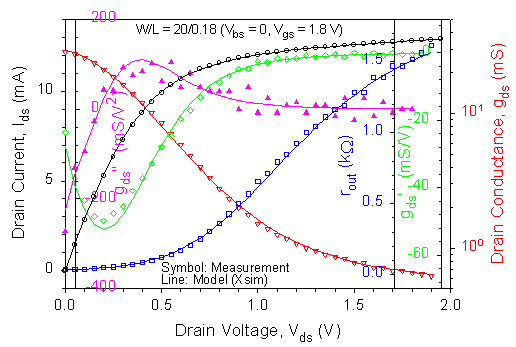
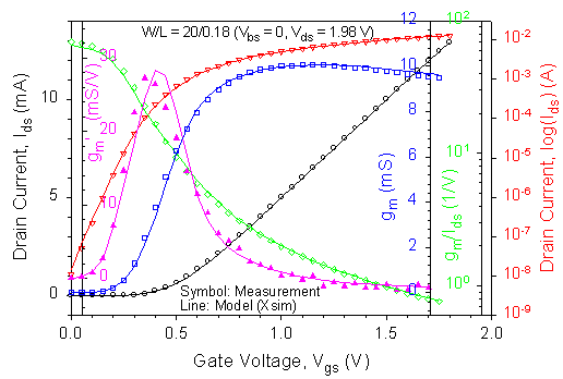
The current Xsim model has been applied to the 0.18-µm technology data, which has 26 fitting parameters with one-iteration extraction using 52 point (I, V) and 13 I-V sweeps of measured data. The predicted results on the 0.18-µm device are shown in Figure 2(a) for Ids - Vds and Figure 2(b) for Ids - Vgs, with the associated higher-order derivatives, in which none of the measurement data was used in parameter extraction.
DOUST Parameter-Extraction Program
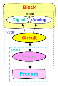
No compact model is complete and useful without a good parameter-extraction strategy. An extraction program, called DOUST (Design and Optimization of Ultra-Small Transistors) [5], is developed for automated extraction and simulation. The calibrated model will be used in the multilevel circuit simulator, called XSIM (see next subsection). The DOUST program has the following functionalities, as shown in Figure 3:
XSIM Multilevel Circuit
Simulator
Accurate transistor compact models are the important building blocks in a circuit simulator. To tradeoff accuracy and speed at the circuit/system level, it is also important to have an engine that is fast, flexible, and extendable. XSIM [6] is designed to be such a single engine to handle analog/digital circuits with automatic and implicit circuit partitioning and mode switching.
XSIM is primarily a SPICE-like analog simulator with vector-sparse matrix solution. It is based on the subcircuit-expansion approach, which results in a �bordered block diagonal� (BBD) matrix that can be efficiently solved [7]. There are two advantages of the subcircuit representation: I) from s modeling viewpoint, when a transistor is modeled as a subcircuit (as opposed to an �element stamp�), it is flexible and extendable to implement device models (especially for RF modeling) as well as reusable (e.g., junction diode model can be used as part of a MOSFET source/drain junctions), and ii) from a matrix-solution viewpoint, when a circuit block (i.e., a logic gate) is expressed as a subcircuit, it provides a natural way for circuit partitioning and dual representation.
The key to the automatic circuit partition is a unified and consistent description of basic logic gates (INV, AND, OR, NAND, NOR, XOR) at two levels of abstraction based on the subcircuit-expansion approach. In XSIM, a new element type, U, is introduced to represent basic logic elements, which has two representations: I) As a logic element, it parallels a circuit element (such as a MOSFET, M) with an associated logic technology description that parallels a transistor technology description (.model card) with a model type logic and the model parameters. ii) As a subcircuit, it consists of the full transistor circuit that makes up the gate (.subckt card). With this dual representation, the logic-level parameters (such as delays, rise/fall times) can be consistently characterized by a full simulation of its subcircuit. Circuit partition for analog and digital parts becomes automatic without the need for an auto-partitioner and, in particular, this partition can change during a simulation.
Because of the dual representation of a logic gate, the mode in which each logic gate is simulated can be I) analog (full circuit simulation as if the U element is replaced by an X subcircuit call), ii) digital (event-driven Boolean function evaluation plus delays), or iii) mixed (switching between �analog� and �digital� modes is determined by the simulator at run time based on the quality of the input signal to each gate). A number of switching criteria can be specified, such as voltage levels fall out of the logic-level range, rise/fall time is larger than certain margin, etc. Given that both analog and digital modes exist, the decision for which mode to use is made for each logic element, and at run time. Hence, both circuit partitioning and mode switching are implicitly done by the simulator without the need for the user to predetermine before a simulation. This is particularly useful for mixed analog/digital circuits, which can be simulated at different levels of abstraction, with �digital speed� whenever possible and �analog accuracy� wherever necessary.
With the logic-element subcircuit representation, it is possible to precalculate the input/output capacitances, the rise/fall delays and rise/fall times at various conditions (such as different loading capacitance, input transition time, and single/all-input triggering) by a full-subcircuit simulation for each basic logic gate, and store the calculated parameters with the associated logic model card. The XSIM data structure allows any element types to be traced for any given user circuit netlist, thus, the fanout capacitance of each gate can be determined at run time. The dynamic-delay model [8] will interpolate the actual delays (and rise/fall times) from the stored logic-parameter table based on the actual fanout, input transition time, and number of triggering at run time.
Logic model precharacterization and library generation have all been automated in XSIM. The XSIM command �.extract <file.cfg>� will generate all logic models in the configuration file, <file.cfg>, which contains all the basic logic gates (U) and their subcircuits, and store them in a library file, <file.lib>. The library file can be included in a user circuit netlist, <file.ckt>, using the command �.library <file.lib>�. During a simulation session, if the user temporarily changes the logic gate description, XSIM will generate the new logic model on the fly without affecting the characterized library files.
One example of XSIM mixed-mode simulation is a 4-bit full adder implemented in the NAND-NAND logic. The full adder consists of 224 transistors and, when simulated in �digital� mode, a total of 48 logic gates. The inputs are ideal voltage pulses with a simulation time step of 0.5 ns. The �COUT� port (carry bit of the last stage) has the largest delay at 8 gate delays. Results are reported in Table 1. Also shown is the XSIM�s unit-delay (UD) model in which the rise and fall delays are fixed at 1 ns. A large accumulated timing error is observed for the UD model as compared to the dynamic-delay (DD) model, which has a comparable speed. The DD model runs three times as fast as its �analog� mode as well as HSPICE and Timemill, and is more accurate than the Timemill�s table-lookup method. In �mixed� mode, XSIM improves its accuracy over the DD model, but is slower than in �analog� mode. This is due to the special case for this circuit in which most of the gates did not switch to digital mode during the simulation, and there is overhead for the mode switching. For circuits with a large portion of digital and a small portion of analog components, the �mixed� mode capability of XSIM should prove to be beneficial in speed-accuracy tradeoff.
Model Extension
The compact model (Xsim) and the circuit simulator (XSIM) discussed thus far have been centered on the device/circuit level. In order to link process effects to system performance, the current framework needs to be �pushed down� to correlate to true process variables (e.g., implant dose/energy, oxidation time/temperature) and �extended up� to handle system blocks with analog, digital, and mixed-signal functionalities. With our consistent dual representation and single-engine implementation, it has the advantage over programs created by separate development groups. A schematic block diagram of our implemented/proposed multilevel modeling environment is shown in Figure 4.
Technology-Level Correlation
As our CM is physics based with separation of physical and fitting parameters, it is possible to vary physical parameters around the fixed (average) process fitting parameters to study process fluctuation effect on electrical performance captured by the CM. The other approach is to correlate fitting parameters to true process variables based on split-lot data, which has been exploited for implant dose and energy [5]. A sample result for the 0.25-µm technology prediction is shown in Figure 5, in which the threshold-voltage versus gate length (Vt - L) is calibrated with wafer number 15 data and, with a correlation to the long-channel doping of wafers 17 and 19. The Vt model with an implant dose as input shows excellent prediction of the other split-lot wafer data (17, 18, 19). With the internal subcircuit expansion of a transistor, it is possible to explore such capabilities for RF/noise modeling at the circuit-element level rather than using user subcircuits. Finally, combined with a calibrated TCAD, our Xsim/DOUST/XSIM program is expected to provide a quick and reliable guide to technology developers as well as accurate skew models for circuit designers.
Block-Level Modeling
Analog functional blocks (e.g., op-amp) can usually be simulated in two ways: full circuit (using transistors and circuit elements) or behavioral (using mathematical functions). XSIM supports internal built-in behavioral functions (for circuit elements) in the SPICE-netlist format. The motivation to have a block-level representation is for �analog acceleration,� i.e., to simulate subsystems at a higher level of abstraction. Applying the same idea as the U element for a logic gate for digital acceleration, it is proposed [6, 8] to have a P element for a circuit block for analog acceleration, which also has a dual representation for subcircuit/block. The high-level block can be a function or lookup table that corresponds to the subcircuit, which allows specified blocks in a large circuit to be simulated at the desired level of abstraction. Finally, interconnect models can be treated in a similar way as part of a unified hierarchical model for a given system.
The idea of the above multilevel representation is illustrated in Figure 6.
Conclusions
As listed in the 2001 edition of the International Technology Roadmap for Semiconductors [9], one of the difficult challenges beyond 2007 (< 65 nm) in modeling is Software Module Integration--�seamless integration of simulation modules with focus on interplay and interfacing of the modules in order to enhance design effectiveness.� And one of the examples is �a complete simulation chain linking process modeling, device modeling, compact model extraction, and library generation.� Historically and currently there have always been dedicated groups developing comprehensive advanced device models and efficient matrix-solution techniques to be implemented in circuit simulators. However, there is a missing link between the model developers and circuit-simulator vendors as well as between the technology developers and circuit designers. The recent development of model-simulator interface using Automatic Device Model Synthesizer (ADMS) and Verilog-A (as presented in [10]) attempts to address this issue. However, there are still problems associated with standardization, efficiency, extraction, and model support (version control). The key to establishing such a link lies in the development of a single-engine tool that is built with this express goal. The proposed modeling framework in this article (and the related developments) represents our vision and implementation toward such a goal.
Acknowledgments
The author wishes to thank Chartered Semiconductor Manufacturing Ltd. and LSI Logic Corp. for their continued support of experimental data for our model development.
Xing Zhou is currently an associate professor in the School of Electrical and Electronic Engineering, Nanyang Technological University, Singapore. E-mail: exzhou@ntu.edu.sg.
References
[1] Y.P. Tsividis and K. Suyama, �MOSFET modeling
for analog circuit CAD: Problems and prospects,� IEEE J. Solid-State
Circuits, vol. 29, no. 3, pp. 210-216, 1994.
[2] E.Y. Chou and B. Sheu, �System-on-a-chip design
for modern communications,� IEEE Circuits Devices Mag., vol. 17,
no. 6, pp. 12-17, 2001.
[3] M. Lundstrom and Z. Ren, �Essential physics of
carrier transport in nanoscale MOSFETs,� IEEE Trans. Electron Devices,
vol. 49, no. 1, pp. 133-141, 2002.
[4] R.L. Pritchard, �Transistor equivalent circuits,�
Proc.
IEEE, vol. 86, no. 1, pp. 150-162, 1998.
[5] http://www.ntu.edu.sg/home/exzhou/Research/DOUST/pub.htm
[6] http://www.ntu.edu.sg/home/exzhou/Research/XSIM/pub.htm
[7] A.T. Davis, �Implicit mixed-mode simulation of
VLSI circuits,� Ph.D. thesis, Univ. of Rochester, New York, 1990.
[8] T. Tang, �Mixed-mode analog-digital circuit simulation,�
M.Eng. thesis, Nanyang Technological University, Singapore, 1997.
[9] http://public.itrs.net/
[10] http://www.nanotech2003.com/WCM2003.html
Table 1
Speed and Accuracy Comparison of the
4-Bit Full Adder.
|
|
|
|
|
||
|
|
|
|
|||
|
|
|
|
|
|
|
|
|
|
|
|
|
|
|
|
|
|
|
|
|
|
|
|
|
|
|
|
|
|
|
|
|
|
|
|
|
|
|
|
|
|
|
|
|
|
|
|
|
 (a)
(a)
 (b)
(b)
2. Xsim predicted results on the 0.18-µm device for (a) Ids
- Vds and (b) Ids - Vgs, with the associated
higher-order derivatives.
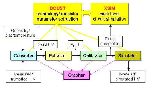
3. DOUST parameter-extraction program.
4. XSIM multilevel circuit-simulation environment.
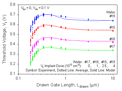
5. Xsim predicted Vt - L from wafer split-lot
with implant dose as input.
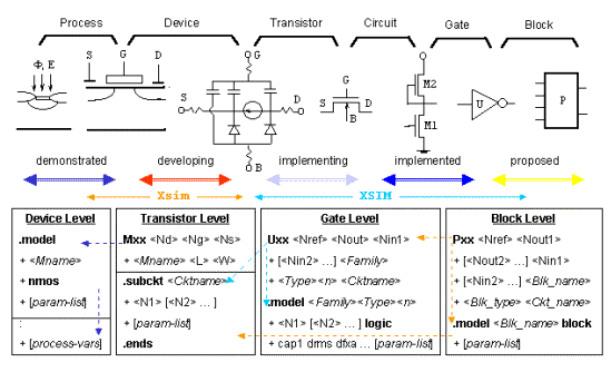
6. Multilevel modeling with dual representation: from process through
device/circuit to system.