Project DOUST (Design and Optimization of Ultra-Small Transistors) is initiated with the express motivation of constructing a framework that segments the design and optimization of ultra-small transistors. The purpose of the conceptual framework is to provide an efficient and cost-effective aid to new technology development and transistor design and optimization.
This project has started as a joint project between Nanyang Technological
University (NTU) and Chartered Semiconductor Manufacturing Ltd. (CSM) in
the context of the 0.18-µm CMOS process technology to be developed
by CSM.
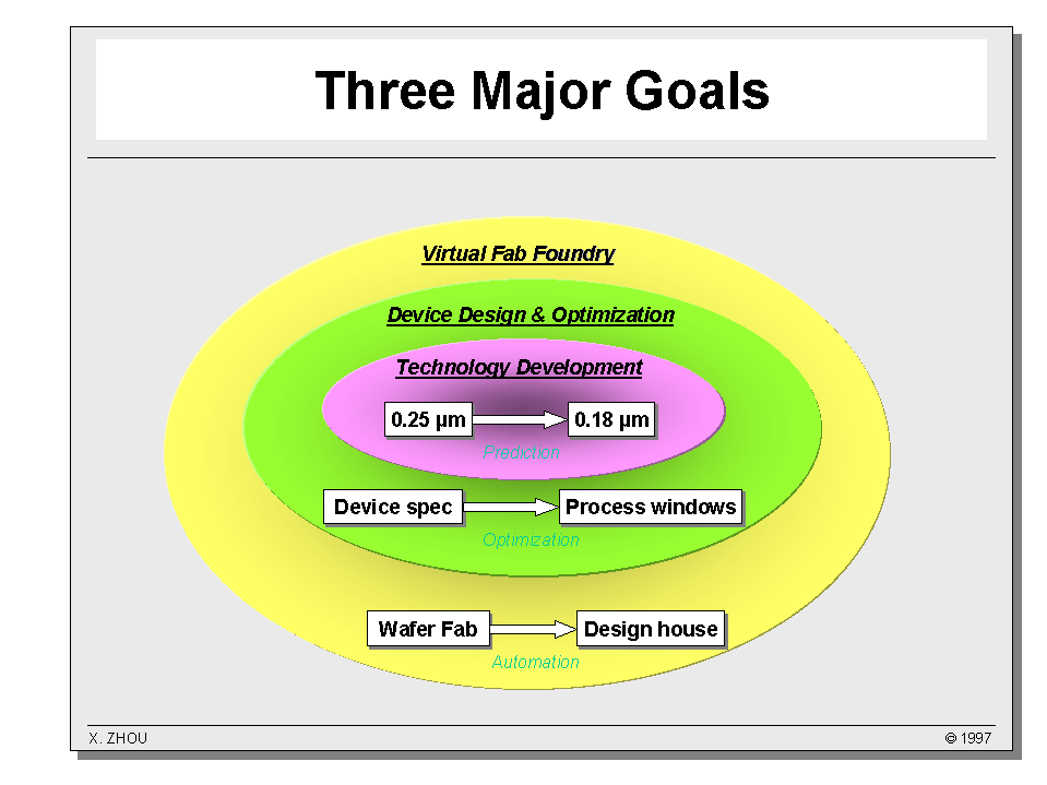
There are three major goals for Project DOUST. For immediate interests, it is aimed at predicting the 0.18-µm technology to be developed based on a TCAD-calibrated VWF technology from an existing 0.25-µm technology. To a larger extent, a framework will be constructed to aid ultra-small transistor design and optimization by providing process windows for a given set of device performance specifications. Ultimately, this project will be a first step towards the establishment of a virtual fab foundry (VFF) to bridge the gap between the wafer fab and the design house.
Specific objectives as set out by the joint project are listed below:
The conceptual framework is based on the process database and the device database constructed from the TCAD simulations. Suppose, for example, there are q process targets, each one is a function of one or more of the p process variables; and there are v device targets, each one is a function of one or more of the u device variables. In many cases, a process target is also a device variable (e.g., tox, Leff, xj).
The conceptual framework will be able to link the device targets to
the process variables. This means that two types of information (plots)
can be obtained: (1) Design curve in which one or more device targets
can be plotted against one major process variable and, optionally, with
a secondary process variable as a parameter for comparison. (2) Process
box in which contours of one or more device targets can be plotted
against two major process variables. The design curves and the process
boxes can be very useful in aiding technology development and multi-target
transistor optimization.
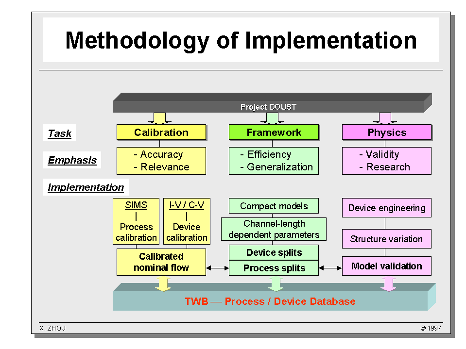
Project DOUST is to be implemented with three tasks in parallel: calibration, framework, and physics, with different emphasis for each task.
Calibration work aims at the accuracy of the simulator models and the relevance of the simulation results. Physics study mainly concerns with the validity of the process/device models being used, since we are pushing to the limit of our current understanding. For the framework design, however, the focus is mainly on the efficiency and generalization. Of course, the usefulness of the developed framework depends on how well we calibrate the models (accuracy) and how well we understand the device physics (validity).
Implementation of the above three tasks can be carried out in parallel, with close interaction among them. Everything will be based on the 0.25-µm CMOS process being developed at CSM. Process simulator will be calibrated to the SIMS measurements, and device simulator will be calibrated to the measured IV and CV characteristics. An up-to-date calibrated nominal flow will be made available for other tasks. Device-model validation will be studied with different structures and biasing conditions, and the results will be fed back to the other two modules. Research on device engineering (e.g., channel doping and drain engineering) will also be conducted. A framework will be constructed by running extensive process and device splits to build the process and device databases. Channel-length dependent parameters will be extracted from the database to provide a guide for technology scaling. Compact models for the targetvariable dependencies will be developed. The information will be shared among the three modules through the process/device database under the TMA WorkBench (TWB).
Eventually, given a more accurately calibrated model, or a new process
recipe, the framework should be able to generate a new database, the process
windows to bracket the final optimum design, and the compact models as
an efficient design guide, all within the region of validity of the models
used.
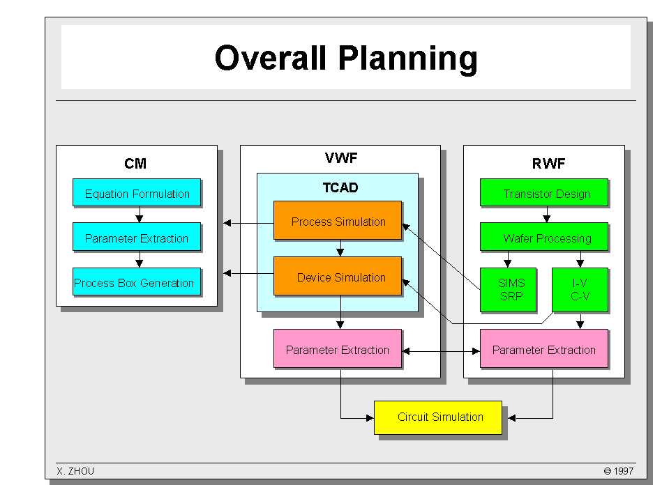
There are three major modules in the overall planning for Project DOUST:
Virtual Wafer Fab (VWF), Real Wafer Fab (RWF), and Compact
Modeling (CM). It is centered at the core TCAD environment --
process and device simulations. The VWF module forms a self-contained
system, from process specification to circuit parameter extraction, which
is in parallel with the RWF module. Comparison of circuit performance
between the VWF and RWF modules can be made at the transistor level or
at the circuit level through SPICE circuit simulation. The RWF module
provides experimental data to be used in process/device simulator calibration
as well as verification of the developed technology and the compact model.
The CM module depends on the TCAD results, and it provides a first attempt
at formulating higher-level modeling of processdevicecircuit inter-dependencies
from a lower-level model.
When we look at the current status of the EDA industry as well as the
chip design and fabrication practice, three trends can be observed.
First, design house and wafer fab are relatively independent of each other,
but there is an increasing need for coupling and information exchange between
the two. Secondly, most existing ECAD tools do not take into consideration
of the real (gate and interconnect) delay information from the actual transistor
structure and layout, and it is increasingly important to consider these
effects at the early stage of a design. Finally, although the TCAD
approach to transistor design and technology development is becoming popular,
it is mainly restricted to R&D groups and semiconductor companies,
and there is a barrier for the general CAD tool users since use of these
TCAD tools requires advanced knowledge of process and device physics.
In fact, TCAD vendors are already beginning to provide professional services
to customers for calibration and efficient use of their tools.
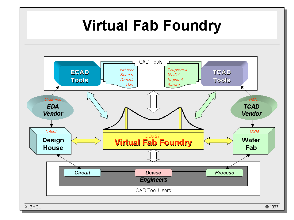
The idea of the virtual fab foundry is to bridge the gap between the design house and wafer fab, to link ECAD tools with TCAD information, and to provide services to the CAD tool users. Project DOUST is a first step towards the establishment of such a foundry. Take the local design house, Tritech, and the wafer fab, CSM, as an example. Suppose a Tritechs design is to be fabricated by CSM. Based on the robust database the virtual fab foundry has implemented and calibrated to the CSMs technology, a set of SPICE and interconnect delay parameters could be generated and provided to Tritech even before the design is fabricated. Even designs using new technologies, which have not been developed, can be predicted. Other important information, such as statistical SPICE parameters due to process variations, can also be generated from the virtual fab foundry.
Ultimately, successful implementation of the VWF technology could lead
to the general services to the chip design and fabrication industry with
the idea of internet-based TCAD.
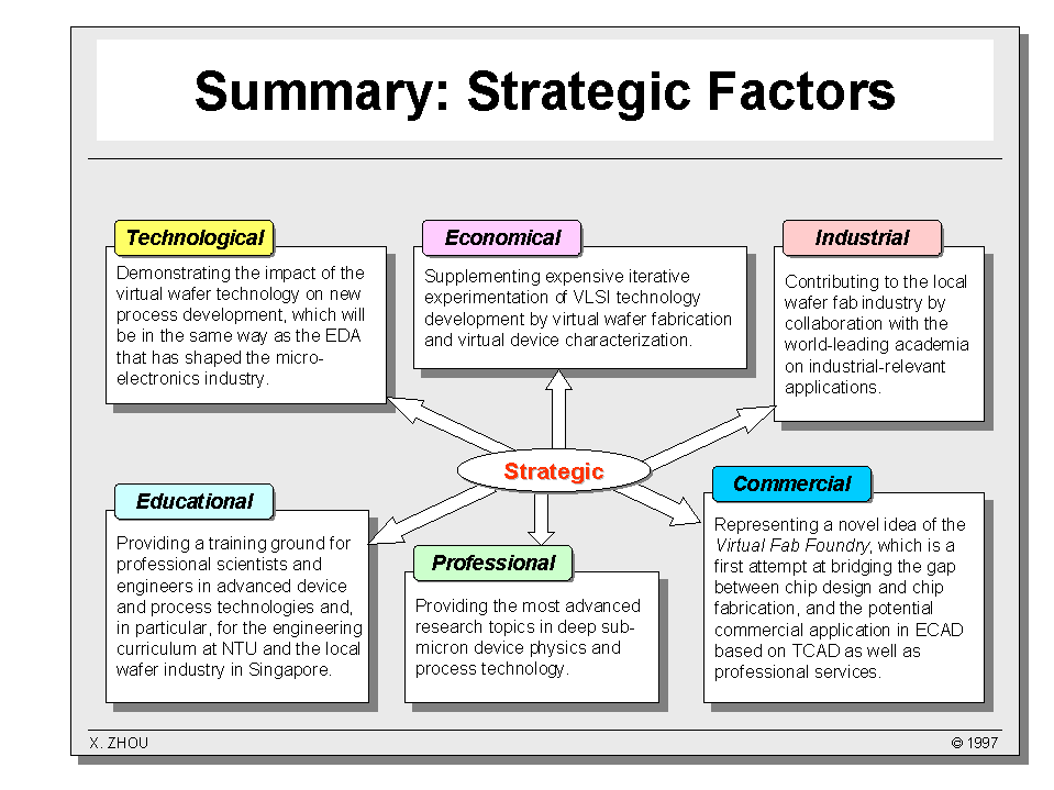
In summary, the proposed Project DOUST has the following strategic factors: