Xing Zhou, Siau Ben Chiah, and Khee Yong Lim
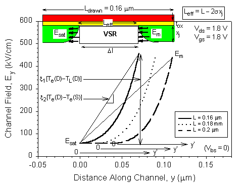
Fig. 1 Channel lateral field (y' axis) from quasi-2D solution for three devices at Vds = Vgs = 1.8 V (based on the extracted model from the given technology data). L = Ldrawn is the drawn gate length, Leff = L - 2sxj is the effective channel length, in which the lateral-diffusion parameter s is extracted together with Vt [11].
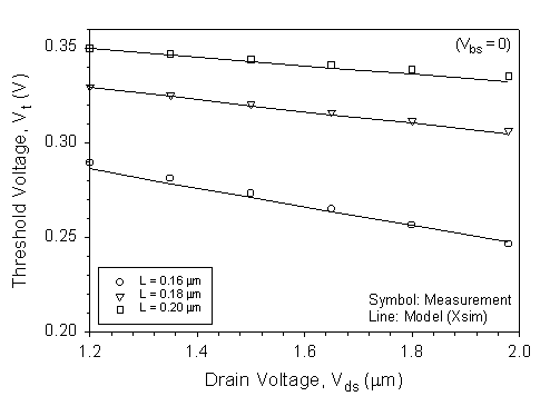
Fig. 2 Measured Vt - Vds curves (symbols) for three short-channel devices compared with model prediction (lines) showing excellent DIBL modeling.
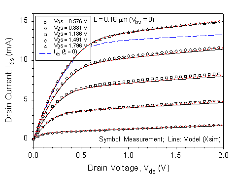
Fig. 3 Measured (symbols) and modeled Ids - Vds curves for the 0.16-mm device for model Eq. (5)(a) (dotted lines) and model Eq. (5)(a)+(b) (solid lines). The Ids model (without CLM) is plotted by the dashed line.
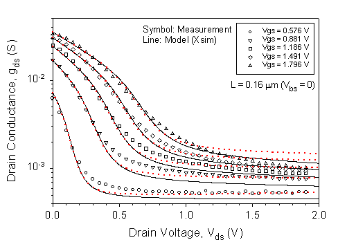
Fig. 4 Measured (symbols) and modeled gds - Vds curves for model Eq. (5)(a) (dotted lines) and model Eq. (5)(a)+(b) (solid lines) directly obtained from numerical differentiation of the curves in Fig. 3.
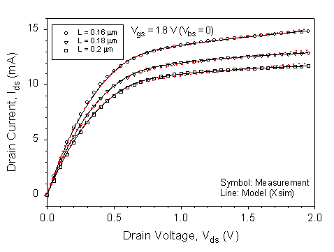
Fig. 5 Measured (symbols) and modeled Ids - Vds curves for three devices for model Eq. (5)(a) (dotted lines) and model Eq. (5)(a)+(b) (solid lines).
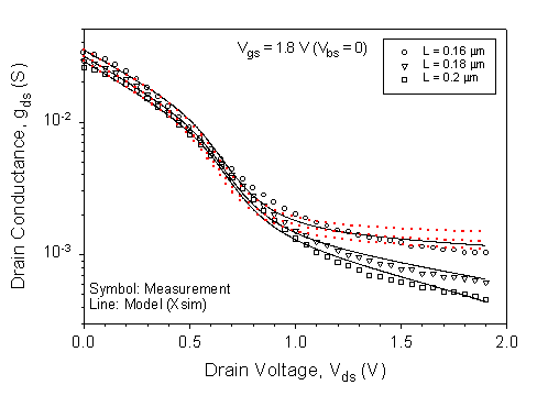
Fig. 6 Measured (symbols) and modeled gds - Vds curves for three devices for model Eq. (5)(a) (dotted lines) and model Eq. (5)(a)+(b) (solid lines) from numerical differentiation of the curves in Fig. 5.