Fig. 1 | Fig. 2 | Fig. 3 | Fig. 4 | Fig. 5 | Fig. 6 | Fig. 7 | Fig. 8 | Fig. 9 | Fig. 10 | Fig. 11 | Fig. 12
Xing Zhou, Member, IEEE, Tianwen Tang, Lee Seng
Seah, Chong Jin Yap,
and Seok Cheow Choo,
Member, IEEE
Fig. 1 | Fig. 2 | Fig. 3 | Fig. 4 | Fig. 5 | Fig. 6 | Fig. 7 | Fig. 8 | Fig. 9 | Fig. 10 | Fig. 11 | Fig. 12
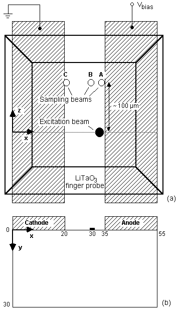
Fig. 1 (a) Top view of sample and measurement setup for the silicon edge-illumination experiment. (b) Cross-sectional view which is the simulation region.
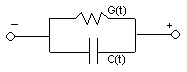
Fig. 2 Equivalent circuit model of the transmission-line photoconductor consisting of a time-varying conductance in parallel with a gap capacitance.
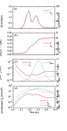
Fig. 3 (a) Total terminal current (solid line) and equivalent gap conduc-tance (dotted line) calculated from Eq. (6); (b) terminal charge (solid line) and equivalent gap capacitance (dotted line) calculated from Eq. (7); (c) dielectric relaxation times calculated from Eq. (9) (solid line) and Eq. (8) (dotted line), and photocarrier generation rate (dashed line) (charge per 10-fs time interval); (d) replot of the data in (a) and (c) (Gphoto) on a logarithm scale.
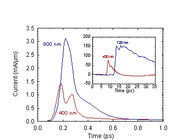
Fig. 4 Total terminal current for two excitation wavelengths, 400 and 800 nm. The measured electro-optic signal (probed at point B in Fig. 1) for two wavelengths as indicated is shown in the inset.
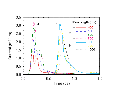
Fig. 5 Total terminal current for different wavelength photoexcitations. Group b curves have been shifted in time by 0.5 ps to avoid clustering of curves.
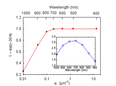
Fig. 6 The function F(a) = 1 - e-30a, which is proportional to the total number of generated carriers, is plotted against a, the absorption coefficient, showing two distinct regions from which the effect of light penetration can be separated from that due to the total generated carriers. Inset: peak current (extracted from Fig. 5) as a function of wavelength.
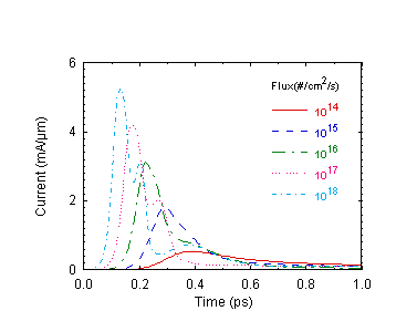
Fig. 7 Total terminal current for different photon flux as indicated for l = 800 nm.
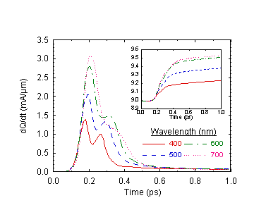
Fig. 8 Time derivative of the terminal charge (shown in the inset) for l = 400, 500, 600, and 700 nm.
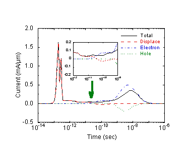
Fig. 9 Terminal current components for an extended simulation of 1 µs after photoexcitation.
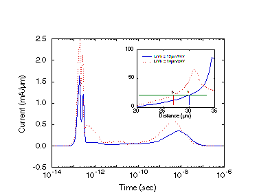
Fig. 10 Total terminal current based on the original structure (solid line) and the scaled one (dashed line). The inset shows the initial (t = 0) surface (y = 0) field across the gap for the two structures. The centers of the excitation spots are labeled by a and b which have the same local-field strength.
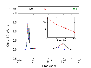
Fig. 11 Total terminal current for different carrier lifetimes as indicated. Inset: derived frequency limit of the laser pulse train as a function of carrier lifetime.
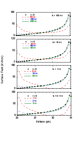
Fig. 12 Snapshots (time frame as indicated in each figure) of
the surface field across the gap for different carrier lifetimes.
The solid lines coincide with the solid circles (initial surface field)
which indicates the time needed for full restoration of the field.