Fig. 1 | Fig. 2 | Fig. 3 | Fig. 4 | Fig. 5 | Fig. 6 | Fig. 7 | Fig. 8 | Fig. 9 | Fig. 10 | Fig. 11 | Fig. 12
Xing Zhou, Member, IEEE
Fig. 1 | Fig. 2 | Fig. 3 | Fig. 4 | Fig. 5 | Fig. 6 | Fig. 7 | Fig. 8 | Fig. 9 | Fig. 10 | Fig. 11 | Fig. 12
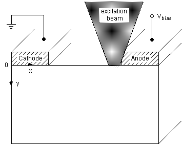
Fig. 1 Sketch of sample and measurement setup for nonuniform gap illumination. The simulation region is the cross section at the excitation spot shown by the enclosed box.
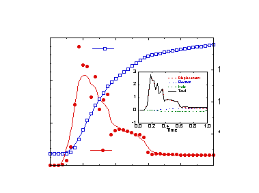
Fig. 2 Total transient terminal current and terminal charge probed at the anode. The current components as indicated are shown in the inset.
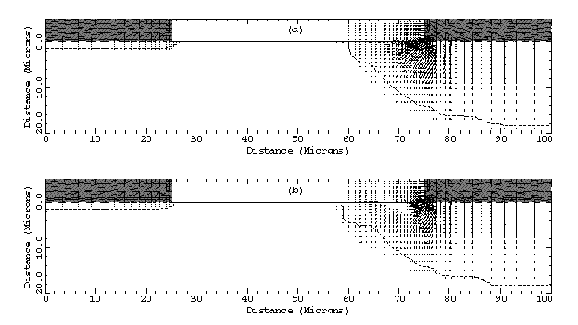
Fig. 3 Displacement-current vectors sampled at (a) t = 0.025, (b) t = 0.2, and (c) t = 1 ps, and conduction-current vector sampled at (d) t = 1 ps. The broken line in each plot shows the edge of the depletion region. (Note: The size of the vectors is relative to each plot itself.)
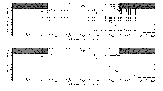
Fig. 4 Field distribution sampled at t = 1 ps.
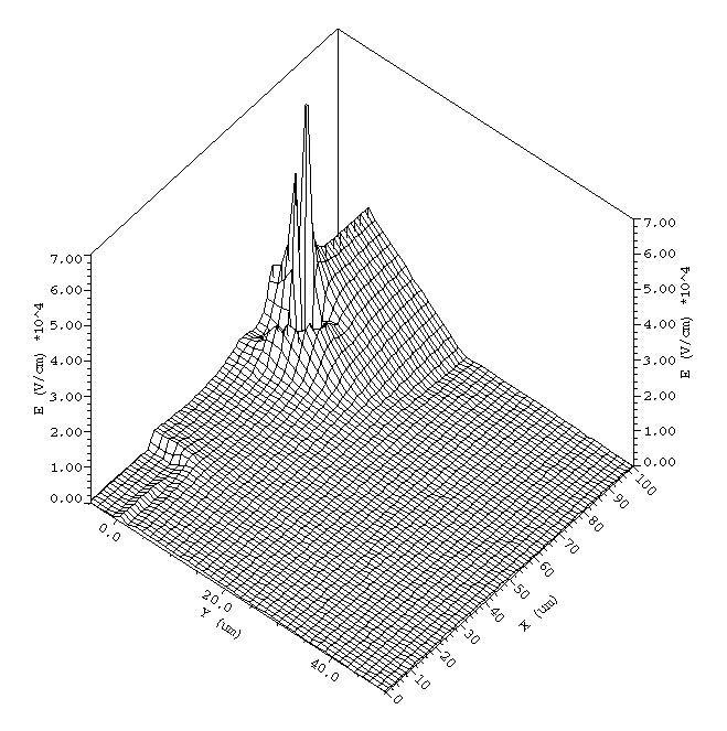
Fig. 5 Surface field across the gap at various instances during the initial transient (time step is 50 fs).
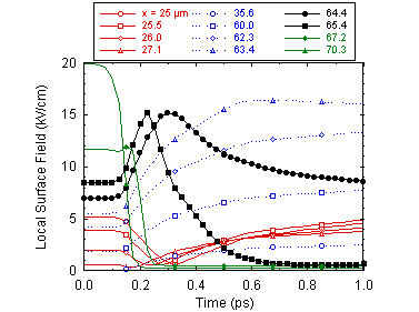
Fig. 6 Time evolution of the local surface field at particular spots across the gap as indicated.
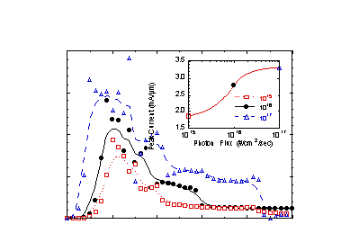
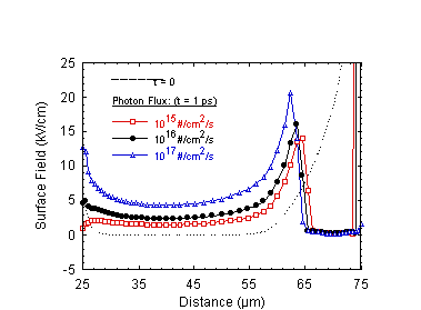
Fig. 7 (a) Terminal-current transient (inset: peak current) for different photon flux. (b) Surface field sampled at t = 0 and 1 ps for different photon flux.
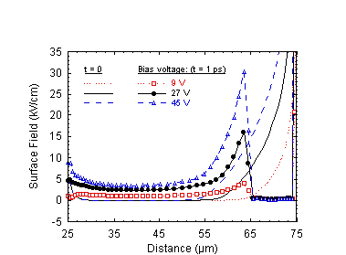
Fig. 8 (a) Terminal-current transient (inset: peak current) for different bias voltages. (b) Surface field sampled at t = 0 and 1 ps for different bias voltages.
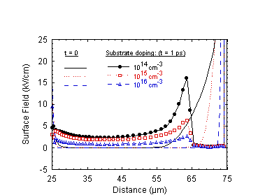
Fig. 9 (a) Terminal-current transient (inset: peak current) for different substrate doping. (b) Surface field sampled at t = 0 and 1 ps for different substrate doping.
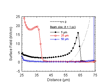
Fig. 10 (a) Terminal-current transient (inset: peak current) for different beam sizes. (b) Surface field sampled at t = 0 and 1 ps for different beam sizes.
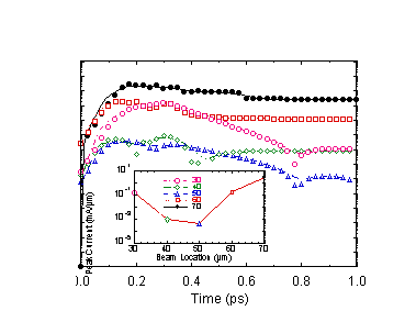
Fig. 11 Terminal-current transient (inset: peak current) for different beam locations across the gap.
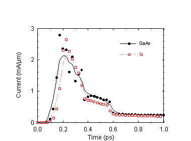
Fig. 12 Terminal-current transient for Si (open square) and GaAs
(solid circle) substrate.
 (a)
(a)
 (b)
(b)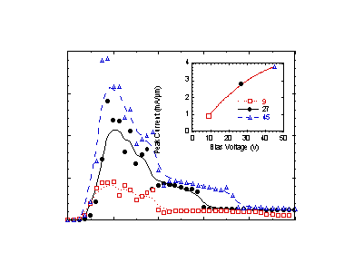 (a)
(a)
 (b)
(b)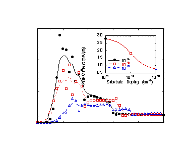 (a)
(a)
 (b)
(b)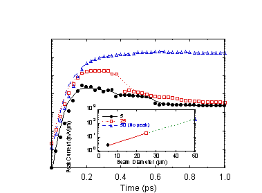 (a)
(a)
 (b)
(b)