Fig. 1 | Fig. 2 | Fig. 3 | Fig. 4 | Fig. 5 | Fig. 6 | Fig. 7 | Fig. 8 | Fig. 9
Tianwen Tang* and Xing Zhou
*Department of Electrical Engineering, University of Rochester, Rochester,
NY 14627
School of Electrical & Electronic Engineering, Nanyang Technological
University, Nanyang Avenue, Singapore 639798
Fig. 1 | Fig. 2 | Fig. 3 | Fig. 4 | Fig. 5 | Fig. 6 | Fig. 7 | Fig. 8 | Fig. 9
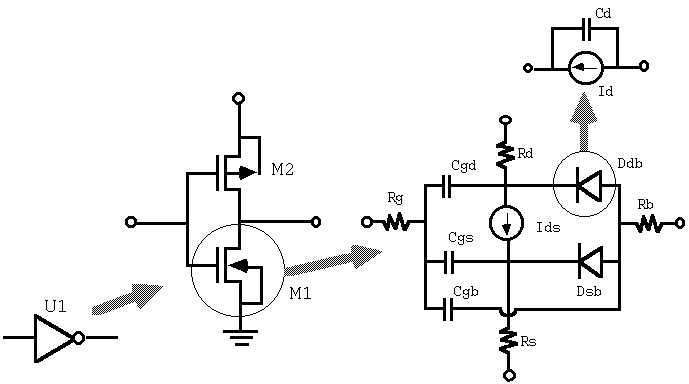
Fig. 1 Subcircuit expansion approach to multi-level logic/transistor modeling.
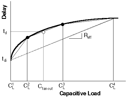
Fig. 2 Piece-wise linear approximation of nonlinear capacitive loading effect and delay interpolation.
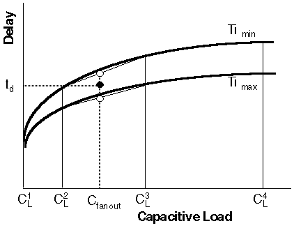
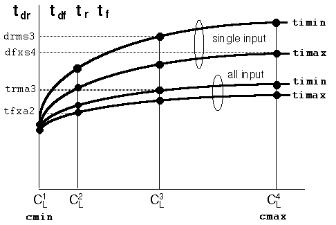
Fig. 3 Delay characterization at min./max. input transition time and dynamic delay calculation by interpolation.
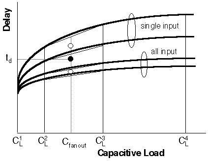
Fig. 4 Delay characterization for single-/all-input triggering and dynamic delay calculation for multiple-input gate.
Fig. 5 Logic parameter extraction for rise/fall delays and rise/fall times.
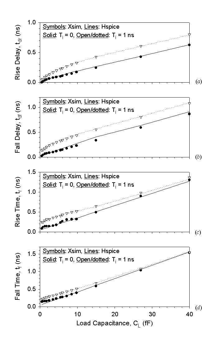
Fig. 6 Xsim characterized delays (symbols) of a 1.2-µm CMOS inverter with signals of Ti = 0 and 1-ns input transition times, compared with the Hspice results (lines).
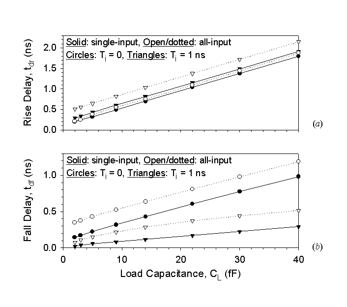
Fig. 7 Characterized delays of a 3-input NOR gate triggered by single- and all-input signals at two input transition times.
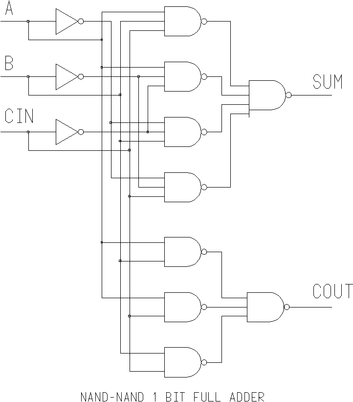
Fig. 8 (a) 4-bit ring counter, (b) block subcircuit, and (c) logic-gate subcircuit.
 (b)
(b)
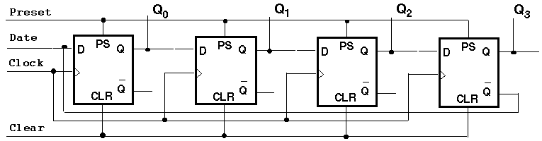 (a)
(a)
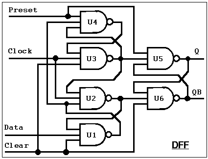 (b)
(b)
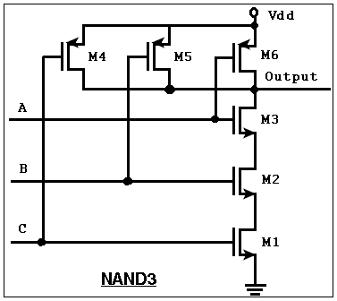 (c)
(c) (a)
(a)