Xing Zhou*, Siau Ben Chiah*, and Khee Yong Lim
* School of Electrical & Electronic Engineering, Nanyang Technological
University, Nanyang Avenue, Singapore 639798
Phone: (65) 790-4532. Fax: (65) 791-2687. Email:
exzhou@ntu.edu.sg
Chartered Semiconductor Manufacturing Ltd, 60 Woodlands Industrial
Park D, St. 2, Singapore 738406
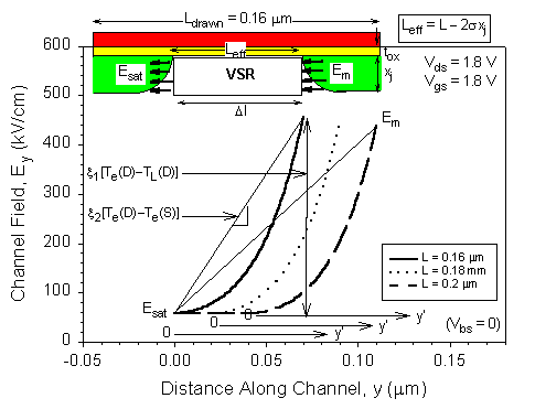
Fig. 1 Channel lateral field (y' axis) from quasi-2D solution for three gate lengths at Vds = Vgs = 1.8 V. VSR lengths (Dl) and Em are all calculated based on the extracted model of the actual devices. Hot-electron effect is evaluated at the drain (y' = Dl) by fitting x1, while the thermoelectric effect is approximated by the average slope of Ey across Leff with a fitting parameter x2.
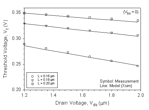
Fig. 2 Measured Vt - Vds (symbols) for three short-channel devices compared with model prediction (lines) showing excellent DIBL modeling.
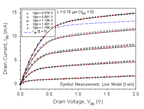
Fig. 3 Measured (symbols) and modeled Ids - Vds curves for the 0.16-µm device for model (4)(a) (dotted lines) and model (4)(a)+(b) (solid lines). The Ids0 model (without CLM) is plotted by the dashed line showing the physics built into our effective Early voltage.
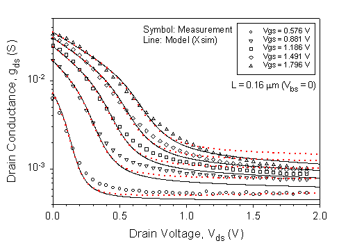
Fig. 4 Measured (symbols) and modeled gds - Vds curves for model (4)(a) (dotted lines) and model (4)(a)+(b) (solid lines) directly obtained from numerical differentiation of the curves in Fig. 3. Improved gds modeling (reduced Ids at increasing Vds) is a result of the thermoelectric effect.
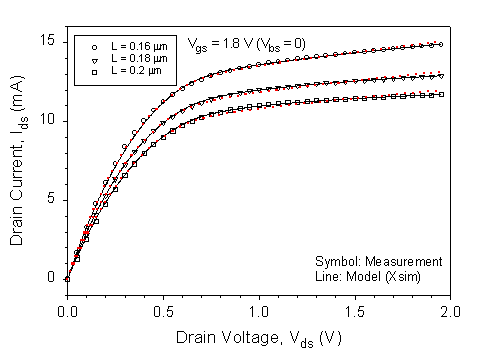
Fig. 5 Measured (symbols) and modeled Ids - Vds curves for three devices for model (4)(a) (dotted lines) and model (4)(a)+(b) (solid lines).
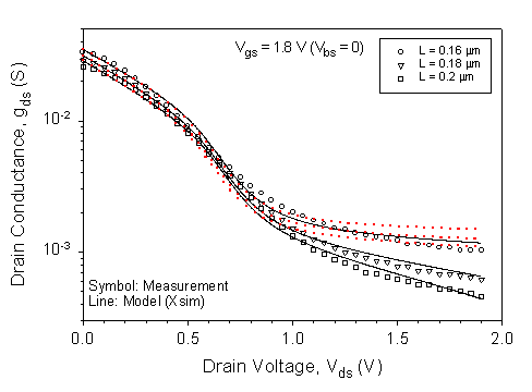
Fig. 6 Measured (symbols) and modeled gds - Vds
curves for three devices for model (4)(a) (dotted lines) and model (4)(a)+(b)
(solid lines) from numerical differentiation of the curves in Fig. 5, showing
gate-length dependence built into the proposed model.