Fig. 1 | Fig. 2 | Fig. 3 | Fig. 4 | Fig. 5 | Fig. 6 | Fig. 7 | Fig. 8 | Fig. 9 | Fig. 10 | Fig. 11
Xing Zhou, Senior Member, IEEE
Fig. 1 | Fig. 2 | Fig. 3 | Fig. 4 | Fig. 5 | Fig. 6 | Fig. 7 | Fig. 8 | Fig. 9 | Fig. 10 | Fig. 11
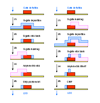
Fig. 1 Two conceptual processes to realize the proposed HMGFET with a length of Ls (S-gate spacer thickness), which require 5 additional steps inserted between gate definition and LDD formation of a conventional (SMG) process with gate length of Lg. The S-gate could be formed by either an asymmetric etch (left) or asymmetric lift-off (right) process.
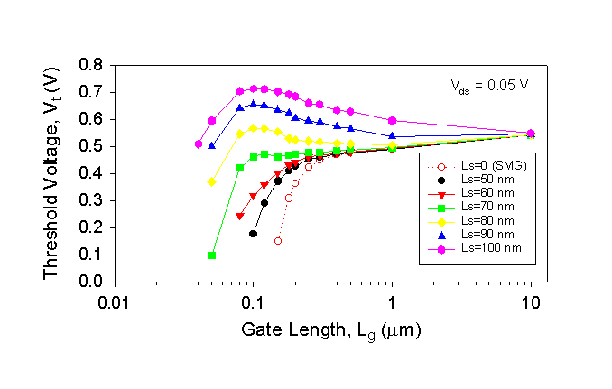
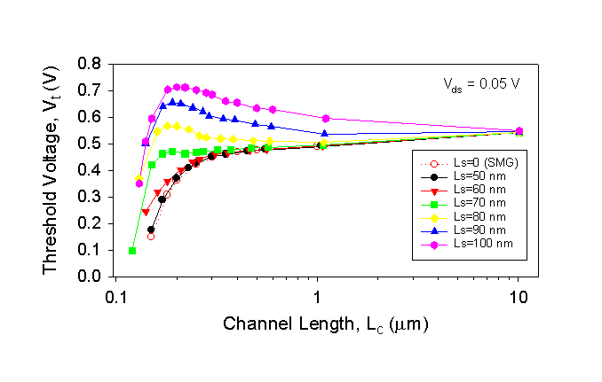
Fig. 2 Linear threshold voltage against (a) gate length or (b) channel length for different values of S-gate length, compared to the SMGFET (dotted line).
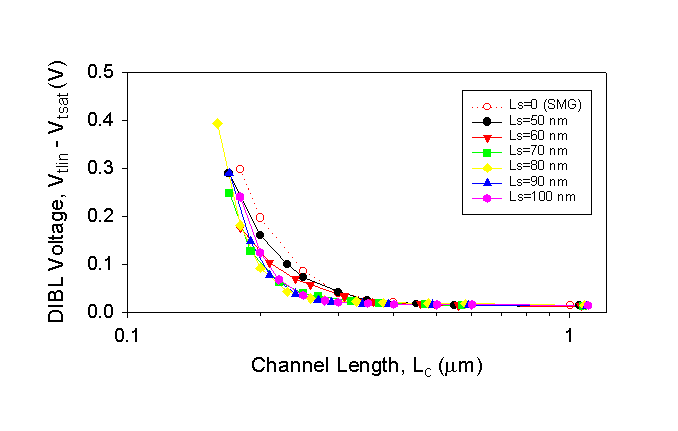
Fig. 3 DIBL voltage against (a) gate length or (b) channel length for different values of S-gate length, compared to the SMGFET (dotted line).
Fig. 4 Leakage current (Ioff) vs. saturation current (Ion) for different values of S-gate length, compared to the SMGFET (dotted line).
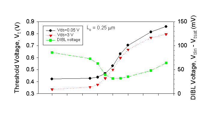
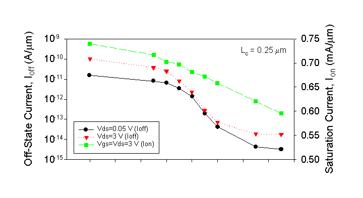
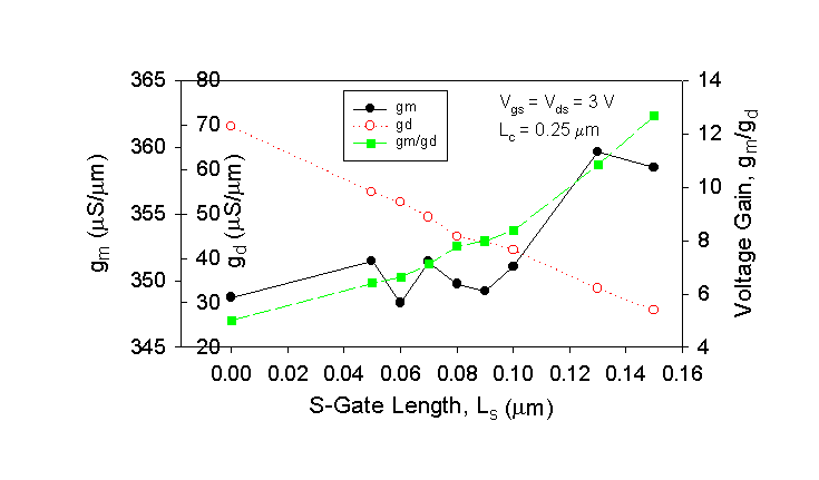
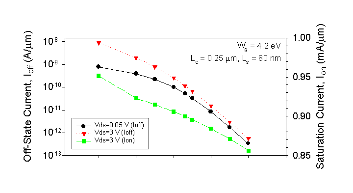
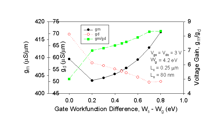
Fig. 5 (a) Linear and saturation threshold voltage and DIBL voltage, (b) saturation and leakage currents, and (c) transconductance, drain conductance, and voltage gain for different values of Ls at a fixed Lc = 0.25 µm.
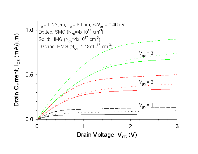
Fig. 6 (a) Ids -Vgs and (b) Ids -Vds characteristics for the HMGFETs with Lc = 0.25 µm, Ls = 80 nm, and Nch = 4x1017 cm-3 (solid lines) or Nch = 1.18x1017 cm-3 (dashed lines), compared to the SMGFET with Lc = 0.25 µm and Nch = 4x1017 cm-3 (dotted lines).
Fig. 7 (a) Linear and saturation threshold voltage and DIBL voltage, (b) saturation and leakage currents, and (c) transconductance, drain conductance, and voltage gain for different values of Ws at a fixed Wg = 4.2 eV for the HMGFET with Lc = 0.25 µm and Ls = 80 nm. The DWsg = 0 case corresponds to the SMGFET with the same Nch = 1.18x1017 cm-3.
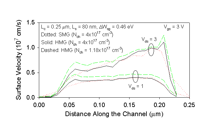
Fig. 8 (a) Electric field and (b) electron velocity along the surface of the channel for the three devices in Fig. 6. The two HMGFETs have Lc = 0.25 µm, Ls = 80 nm, Ws = 4.66 eV, Wg = 4.2 eV, and Nch = 4x1017 cm-3 (solid lines) or Nch = 1.18x1017 cm-3 (dashed lines), compared to the SMGFET with Lc = 0.25 µm and Nch = 4x1017 cm-3 (dotted lines).
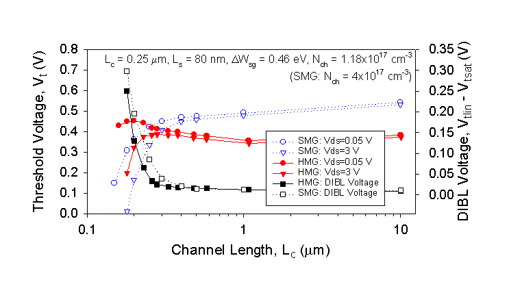
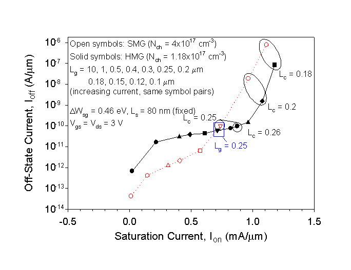
Fig. 9 Linear and saturation threshold voltage and DIBL voltage against (a) gate length or (b) channel length for the HMGFET with a fixed Ls = 80 nm, DWsg = 0.46 eV, and Nch = 1.18x1017 cm-3, compared to the SMGFET (Nch = 4x1017 cm-3).
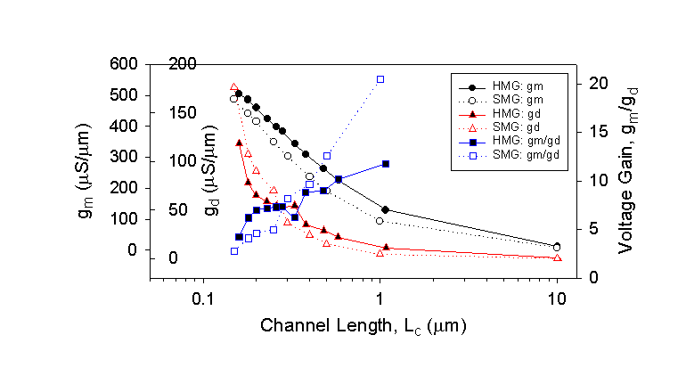
Fig. 10 Transconductance, drain conductance, and voltage gain against (a) gate length or (b) channel length for the same devices as in Fig. 9.
Fig. 11 For the same devices as in Fig. 9, saturation and leakage
currents (shown in the same symbol pair for each Lg)
are plotted (a) as a ratio against gate length, and (b) in pairs.
 (a)
(a)
 (b)
(b)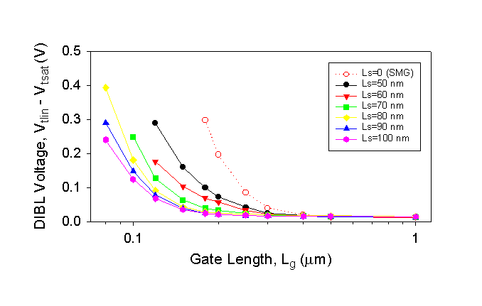 (a)
(a)
 (b)
(b)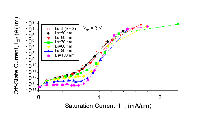
 (a)
(a)
 (b)
(b)
 (c)
(c)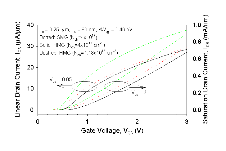 (a)
(a)
 (b)
(b)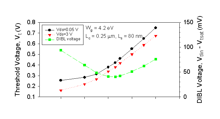 (a)
(a)
 (b)
(b)
 (c)
(c)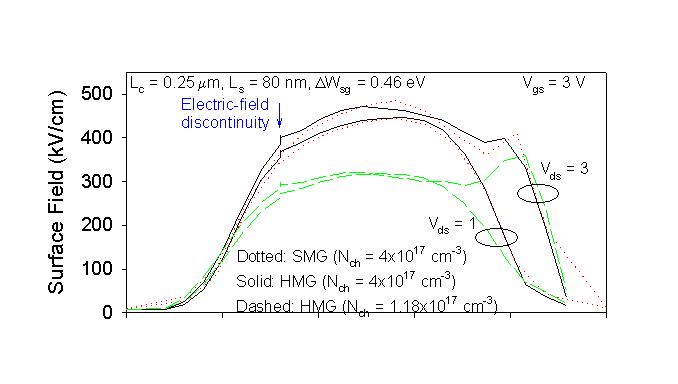 (a)
(a)
 (b)
(b)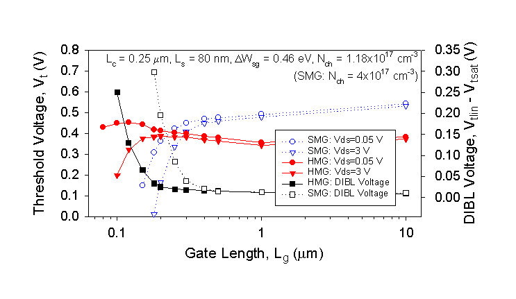 (a)
(a)
 (b)
(b)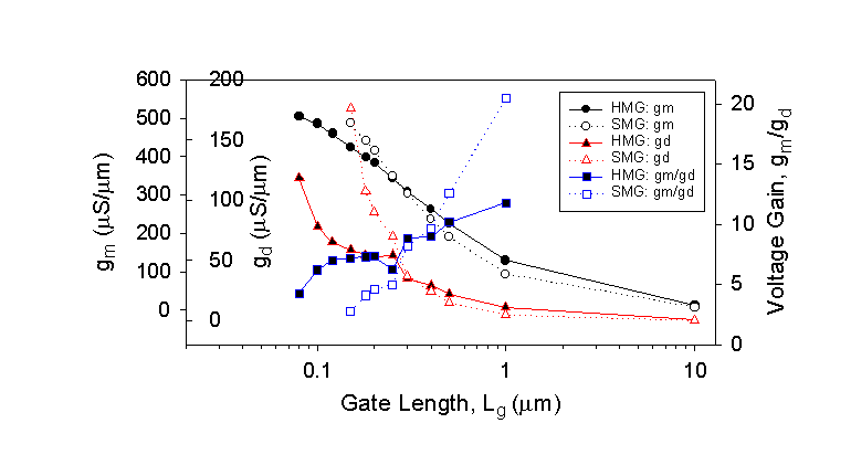 (a)
(a)
 (b)
(b)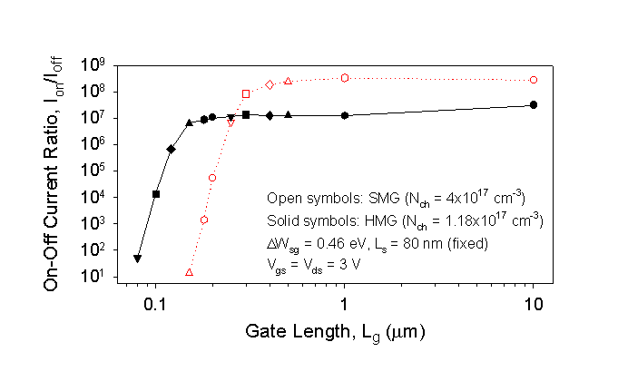 (a)
(a)
 (b)
(b)