| Click on the below links to see the available
lab facilities: < Electromigration Reliability Tester > < High Performance EM system > < Micromanipulator Probe Station > < 4 Point Bend Tester > < Focused Ion Beam (FIB) system > < X-Ray Inspection > < Reactive Ion Etcher (RIE) > < Auto Decapsulation System > < Grinder/Polisher > |
Electromigration
Reliability Tester <back
to top>
The SPC8010 Electromigration Reliability Tester is a high
temperature (350 °C), compact and small volume test system. It
allows you to test, gather data, analyze data and generate
reports to assure the integrity of your process. The system is a
very reliable and stable test system available for package level
electro migration (EM) and time dependent dielectric breakdown (TDDB)
testing. All measurement elements are included as integral
components.
| Application: Copper Electro-migration Test (EM) & Thin Dielectrics Time Dependent Dielectric Breakdown Test (TDDB) testing. |
| Specification: | ||
| Capacity : | 16 samples | |
| Current range : | 0 to 100mA | |
| Temperature Range : | 50 ° C to 350 ° C | |
| Temperature accuracy : | +/-1 ° C from set point |
High Performance EM system
<back to top>
The XACT-810 test system is a high performance electromigration
system for evaluating the quality and reliability of all types of
interconnects in semiconductor products under temperature and
current stress. This system is an in-situ test system, where the
resistance change is monitored continously with a high
measurement resolution.
| Application: Electromigration Test (EM) |
| Specification: | ||
| Capacity : | 64 samples | |
| Current range : | 30µA-300mA | |
| Temperature Range : | 100°C to 350°C | |
| Temperature accuracy: | +/-0.02 ° C from set point |
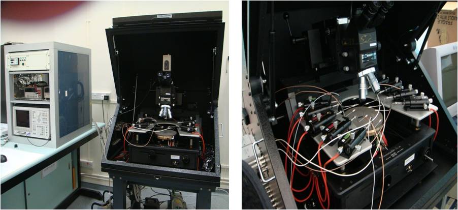
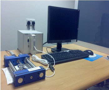
Micromanipulator Probe
Station <back to top>
The 4060 Micromanipulator probe station is a highly configurable
setup for conducting a wide variety of electrical measurements.
Equipped with 8 triaxial probes, this probe station is capable of
achieving accurate and low-noise measurements for characterizing
the electrical properties of nano and sub-micron scale devices.
Reliability testing of devices at the wafer level can also be
conducted using this probe station, which has an integrated
thermal system.
Application:
Nanotechnology, Reliability Testing, Electrical Characterization
of
Advanced Materials & Devices, Low Noise Current & Voltage
Sourcing,
High Resolution Current, Voltage & Capacitance Measurement.
Specification:
Current Source : ±100 fA to ±1 A
Voltage Source : 0 V to ±200 V
fF Measurement Resolution : 1 fA, 1 nV & 5
Standard & Arbitrary Waveform Current Sourcing : up to 100
kHz
Heat control Module : up to 400ºC
Function Generator : up to 20 MHz
Oscilloscope : up to 500 MHz
Light & Electromagnetic Field Shielding
Measurement & Test Devices use:
Agilent 4156 Precision Semiconductor Parameter Amplifier
HP54615B Oscilloscope
Keithley 6221 DC/AC Current Source Meter
Keithley 2400 Source Meter
Keithley Nano Voltmeter
HP 34401 Multimeter
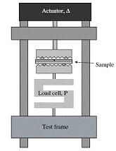
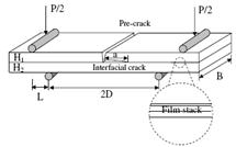
4 Point Bend Tester <back to top>
The Four Point Bend Tester is a customized-built equipment that
is incorporated with a 50 lbf force transducer (actuator), a load
cell and a test frame as shown in the schematic below. The tester
provides capability for testing of the material properties of the
adhesive use for bonding in microelectronics. Hence, the method
is preferred for studies on the adhesion strength of thin films
in semiconductor devices. In the schematic, the sample is placed
between the four load pins and the actuator is programmed by the
DTS, Delaminator Mechanical Test Software to ramp up the
displacement. The force P, from the load at plateau is obtained
in order to calculate the interface fracture energy, Gc.
The actuator can be programmed to ramp up to a maximum load of
200 N.
| Application: Four Points Bending Adhesion Test & DCB (Double Cantilever Beam) |
 |
 |
 |
| Specification: | ||
| ISSM load cells: | 50 lbf / 200 N | |
| Precision linear actuator stroke : | Up to 50 mm | |
| (Min .incremental motion to 0.1 µm) |
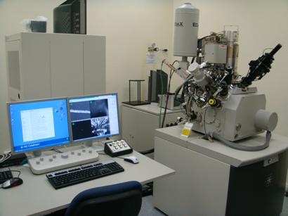
Focused Ion Beam (FIB)
system <back to top>
The FEI Novaetch TM Nanolab DualBeamTM 600i
combines ultra-high resolution field emission scanning electron
microscopy (SEM) and precise focused ion beam (FIB) and
deposition, which becomes a powerful tool for micro-machining, to
modify or machine materials at micro- and nanoscale.
FIB
applications include:
> Cross-sectional imaging through semiconductor devices (or
any layered structure)
> Modification of the electrical routing on semiconductor
devices
> Failure analysis
> Preparation for physical chemistry analysis
> Preparation of samples for transmission electron microscopy
(TEM)
> Micro-machining
> Mask repair
> Non-semiconductor applications
FEI NovaTM Nanolab
DualBeamTM 600i
E-beam
- Voltage: 200 V to 30 kV, continuously adjustable
- Beam Current: < 20 Na
- Resolution: 1.1 nm @ 15 kV, 2.5 nm @ 1 kV
- Detection: in-lens SE and BSE
Ion-beam
- Voltage: 500 V to 30 kV
- Beam Current: 20 nA in 15 steps
- Resolution: 7.0 nm @ 30 kV, 5 nm achievable
Gas Injection System (GIS)
- Platinum Deposition
- Tungsten Deposition
- Insulator Deposition
- Insulator Enhanced Etch
EDAX EDS Detectors
- 10 mm2 2nd power SiLi detector with a resolution of 129 eV (as
measured using the Mn K peak at full width half maximum (FWHM)).
Omniprobe In-situ TEM sample lift-out tool
- In-situ manipulation and motion tools for TEM sample
preparation.
Electrical Feedthrough
- 52 pins electrical feedthrough port allow wire connection
between the sample inside the chamber and the outside multimeters
under high vacuum
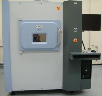
X-Ray Inspection <back to top>
The X-ray Inspection System is used in the field of non-destructive
testing (NDT) for observing and inspecting internal structures
and mounting conditions of modules, sensors, metal castings,
plastics, ceramics and materials alike. The X-ray inspection
system can also be used as a process control and failure analysis
tool to inspect components for the packaging integrity (bonding,
wire opens, wire sweep, die attach etc.); solder joint quality of
components assembled on printed circuit boards or PCBs (especially
Ball Grid Arrays or BGAs and flip-chips for the presence of voids
or cracks).
The high resolution and high magnification system provides a fast
manipulation to the area of interest for quick, distortion-free
and clear inspection, with the mouse-operated control software
"XEVOLUTION". Besides, teaching and step feed functions
are available, which enables repeatable inspections to be
possible.
Several measurements can be performed with the x-ray inspection
system: BGA void measurement, area ratio measurement, dimension
measurement, object measurement and wire sweep ratio measurement.
Shimadzu Micro-Focus X-Ray Fluoroscopic Inspection System
SMX-2000EX
| Spatial resolution: | 1 µm (resolves line and space chart) | |
| Maximum mountable size/ sample weight: | W470 × D420 mm, 5 kg | |
| Maximum inspection area: | X: 460 mm, Y: 410 mm | |
| X-ray tube: | Open tube design | |
| X-ray output: | Max. tube voltage: 160 kV/Max. tube current: 200 µA | |
| Detector: | Flat panel detector, Rotation: ±180°, Tilt: +0 - 70° | |
| System Magnification: | 8,700× |
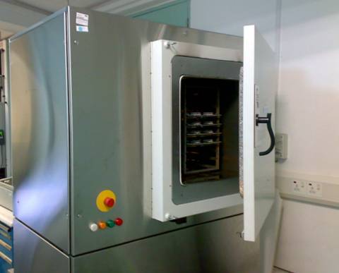
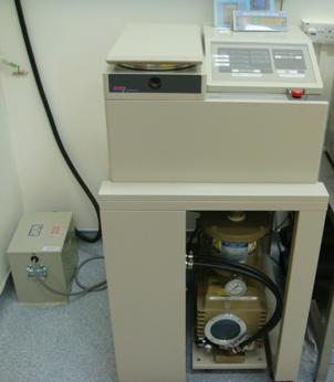
Reactive Ion Etcher (RIE)
<back to top>
The reactive ion etcher is a dry etching system utilising etching
gases such as CF4, O2, or SF6
that provides the plasma for material removal by chemical (free
radicals) and physical (reactive ions) etching. The system is
suitable for removing passivation layers such as Si3N4
and dielectric materials such as SiO2 and
phosphosilicate glass (PSG) of multi-layered integrated circuits
(ICs). Isotropic and anisotropic etching programs can be set as
desired.
ES371 Reactive Ion Etching (RIE) System
| RF power: | 20 – 150 W | |
| High frequency power: | 13.56 MHz | |
| Stage size: | 100 mm | |
| Usable vacuum range: | 80 – 800 mTorr | |
| Usable etching gases: | CF4, O2, SF6, N2, CHF3 | |
| Stage Temperature: | 30 - 70°C | |
| Etching Time: | 0 ~ 99 min | |
| Programming: | 2 steps | |
| Stored recipes: | 98 | |
| Vacuum pump: | Oil rotary pump |
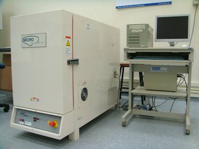
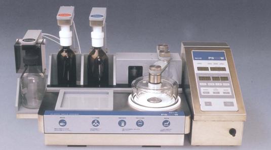
Auto Decapsulation System
<back to top>
The auto or chemical decapsulation is a technique used in failure
analysis to expose the die and bond wires inside a
microelectronic package. This method is suitable if the cause of
failure is physical and can be found on the die or elsewhere
inside the package.
A package is glued (with its front side facing down) onto a
suitable rubber gasket. Rubber gaskets of various sizes for
different package and die sizes are available. The glued package
and rubber gasket are then placed onto a sample adapter or sample
guide for accurate positioning of the area to be exposed. The jet
of acid will rise from the reservoir through the opening of the
rubber gasket to reach the package. Fuming nitric acid, fuming
sulphuric acid or a mixture of both, is usually used to remove
the mold compound of the package to expose the die and the bond
wiresthe . The acid can be heated to a high temperature without
excessively heating the device. In addition, time to decapsulate
can be controlled by the temperature, volume and flow rate of the
acid.
PS102W Plastic Mold Decapsulation System
| Usable acids: | Fuming nitric, fuming sulphuric, sulphuric or mixed acids | |
| Setting temperature range: | Fuming nitric acid: 40 – 80°C | |
| Fuming sulphuric acid: | 40 – 250°C | |
| Mixed acids: | 40 – 250°C | |
| Acid volume setting: | 1 – 50 ml | |
| Flow rate setting: | 2 – 10 ml/min | |
| Decap time setting: | Automatic setting from acid volume/flow rate | |
| Purge gas and pressure: | N2 gas, 0.3 Mpa |
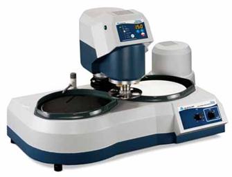
Grinder/Polisher <back to top>
The grinder/polisher is useful for obtaining a metallographic
cross-section to determine the layer structure of a semiconductor
device, for example. Metallographic cross-sections can be
observed under the optical or electron microscopes, for fault
analysis. The grinder/polisher can be used with grinding cloths
with particle sizes ranging from 5 – 269 µm and premium
polishing cloths with particle size ranging from 0.02 – 15
µm. Polishing is becoming increasingly useful in physical
failure analysis or physical deprocessing, when wet etching and
plasma etching are inadequate.
Buehler Beta Twin Series Variable Speed Grinder-Polisher
with Vector Power Head
| General | ||
| Platen speed: | 30 – 600 r.p.m | |
| Platen diameter: | 8-inch (203 mm) | |
| Vector Power Head | ||
| Sample capacity: | Single (1 – 4) | |
| Sample sizes: | 25 mm, 1-inch, 30 mm, 1.25- inch, 32 mm, 1.5-inch, 38 mm, 40 mm | |
| Controls: | Touch pads with LED displays for: On/off, head direction (comp/contra), run/stop, dispenser on/off, time, force (lb/N), water on/off |
|
| Time: | From 30 s – 9 mins 50 s (10 s increments) | |
| From 10 mins – 99 mins (1 min increment) | ||
| Sample force | Single (0 – 15 lbs in 1 lb increment, 0 – 75 N in 5 N increments) | |
| Head speed: | 60 r.p.m | |
| Other features: | Integrated drip-lubricator interface to dispensing system |